UNISOC Unveils T7520 SoC for 5G Smartphones: Octa-Core, 6nm EUV
by Anton Shilov on March 4, 2020 10:00 AM EST- Posted in
- Smartphones
- Mobile
- SoCs
- 5G
- Spreadtrum
- UniSOC
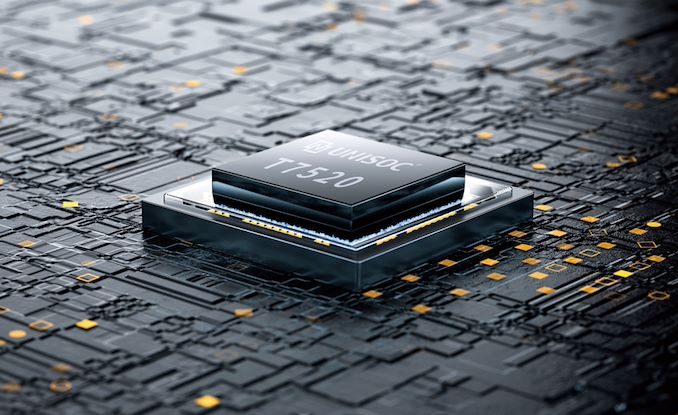
UNISOC, formerly Spreadtrum Semiconductor, has announced its first mobile application processor with an integrated 5G modem. Dubbed the T7520, the SoC also happens to be one of the world’s first chips to be made using TSMC’s 6 nm process technology, which uses extreme ultraviolet lithography (EUVL) for several layers.
The UNISOC T7520 application processor packs four high-performance Arm Cortex-A76 cores, four energy-efficient Arm Cortex-A55 cores, as well as an Arm Mali-G57 GPU with a display engine that supports multiple screens with a 4K resolution and HDR10+. Furthermore, the SoC integrates a new NPU that is said to offer a 50% higher TOPS-per-Watt rate than the company’s previous-generation NPU. In addition, the chip features a four-core ISP that supports up to 100 MP sensors and multi-camera processing capability. Finally, the AP also features the company’s latest Secure Element processor that supports ‘most of crypto algorithms’ and can handle compute-intensive security scenarios, such as encrypted video calls.
One of the key features of the UNISOC T7520 is of course its integrated 2G/3G/4G/5G-supporting modem, which supports 5G NR TDD+FDD carrier aggregation, as well as uplink and downlink decoupling for enhanced coverage. All told, the T7520's modem is designed to offer peak uplink speed of 3.25 Gbps.
The high level of integration of the T7520 SoC is designed to enable smartphone manufacturers to build more reasonably priced 5G handsets, which will inevitably increase their popularity and adoption of the technology. Meanwhile, usage of TSMC’s 6 nm fabrication technology (known as N6) should allow UNISOC to make the AP for less than compared to non-EUV fabrication processes.
UNISOC did not announce when it plans to start shipments of its T7520 application processor, though it is reasonable to expect it to become available this year.
Related Reading:
- Sizing Up The 5G Modem Market: Qualcomm, Intel, Huawei, Samsung, UniSOC, and Mediatek
- CES 2020: MediaTek Announces New Dimensity 800 Mid-Range 5G SoC
- Qualcomm Announces Snapdragon 865 and 765(G): 5G For All in 2020, All The Details
- Qualcomm’s New 3rd Generation Snapdragon X60 5G Modem, Built on 5nm
Source: UNISOC


17 Comments
View All Comments
psychobriggsy - Wednesday, March 4, 2020 - link
Interesting to see a mid-range SoC be made on a leading edge node. Possibly was a 7nm design ported to 6nm, as TSMC's 6nm is compatible with their original 7nm.ksec - Wednesday, March 4, 2020 - link
6nm is considered mainstream by the time it ship, leading edge this year is 5nm.dotjaz - Wednesday, March 4, 2020 - link
6nm is nowhere near leading edge. It's like where 12nm was when 10nm was already out.DanNeely - Wednesday, March 4, 2020 - link
I'm not familiar with the name. Who's used their previous generation SoC?Kvaern1 - Wednesday, March 4, 2020 - link
This is what I get from Google.https://www.kimovil.com/en/list-smartphones-by-pro...
abuzerimsi - Wednesday, November 4, 2020 - link
He's fine at Techindeep. You must follow that place too. https://www.techindeep.com/compare-phoneArsenica - Wednesday, March 4, 2020 - link
Samsung, Panasonic and Chinese brands such as HiSense and Lenovo, usually for low-end China-only devices.Teckk - Wednesday, March 4, 2020 - link
Didn't Intel and Spreadtrum have a license deal sometime? Was that for LTE/5G???ksec - Wednesday, March 4, 2020 - link
Yes. They had the Intel Modem design. Which also meant it is going to be a hint into how Apple's modem will perform.ZolaIII - Wednesday, March 4, 2020 - link
Nope & nope. They had bounded with Intel to use Atoms and use Intel foundery. This almost costed them their existence as nothing good, actually nothing at all ever come from that. 5G modem is the one they developed them self, Intel failed like it did with many other things.