Semiconductors
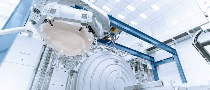
This week ASML is making two very important announcements related to their progress with high numerical aperature extreme ultraviolet lithography (High-NA EUV). First up, the company's High-NA EUV prototype system at its fab in Veldhoven, the Netherlands, has printed the first 10nm patterns, which is a major milestone for ASML and their next-gen tools. Second, the company has also revealed that it's second High-NA EUV system is now out the door as well, and has been shipped to an unnamed customer. "Our High-NA EUV system in Veldhoven printed the first-ever 10 nanometer dense lines," a statement by ASML reads. "Imaging was done after optics, sensors and stages completed coarse calibration. Next up: bringing the system to full performance. And achieving the same results in the...

Intel Process Technology Update: 10nm Server Products in 1H 2020, Accelerated 7nm in 2021
Intel provided an update regarding its upcoming fabrication technologies at its 2019 Investor Meeting. The company is on track to produce server-class products using its 10 nm manufacturing technology...
74 by Anton Shilov on 5/8/2019
TSMC: Most 7nm Clients Will Transition to 6nm
In this week's quarterly earnings conference call, TSMC’s revealed that the company expects most of its 7nm "N7" process customers to eventually transition to its forthcoming 6nm "N6" manufacturing...
39 by Anton Shilov on 5/1/2019
Samsung to Invest $115 Billion in Foundry & Chip Businesses by 2030
Being among the largest contract makers of semiconductors and among leading developers of chips for various applications, Samsung Electronics wants to become the world’s leader in these industries. To...
27 by Anton Shilov on 4/24/2019
GlobalFoundries to Sell 300mm New York Fab to ON Semiconductor
GlobalFoundries and ON Semiconductor on Monday signed a definitive agreement for the latter to buy GlobalFoundries’ 300-mm fab in East Fishkill, New York. In addition to the production facility...
25 by Anton Shilov on 4/22/2019
TSMC: No Plans to Buy Rivals at The Moment
Although TSMC expects demand for chips to increase going forward and despite an ongoing trend towards consolidation on the foundry market, the company has commented that it currently has...
4 by Anton Shilov on 4/22/2019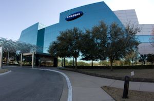
Samsung Completes Development of 5nm EUV Process Technology
Samsung Foundry this week announced that it has completed development of its first-generation 5 nm fabrication process (previously dubbed 5LPE). The manufacturing technology uses extreme ultraviolet lithography (EUVL) and...
21 by Anton Shilov on 4/17/2019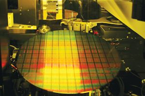
TSMC Reveals 6 nm Process Technology: 7 nm with Higher Transistor Density
TSMC this week unveiled its new 6 nm (CLN6FF, N6) manufacturing technology, which is set to deliver a considerably higher transistor density when compared to the company's 7 nm...
23 by Anton Shilov on 4/17/2019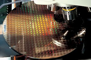
TSMC’s 5nm EUV Making Progress: PDK, DRM, EDA Tools, 3rd Party IP Ready
TSMC this week has said that it has completed development of tools required for design of SoCs that are made using its 5 nm (CLN5FF, N5) fabrication technology. The...
33 by Anton Shilov on 4/5/2019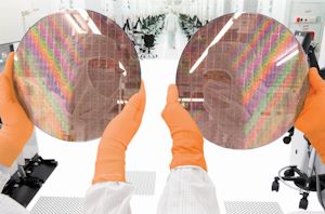
GlobalFoundries and Synopsys Develop Automotive-Grade IP for 22FDX Process Tech
GloalFoundries and Synopsys announced this week that they have jointly developed a portfolio of automotive-gade IP solutions for GF’s 22FDX process technology. The various IP blocks are designed for...
4 by Anton Shilov on 2/22/2019
TSMC’s Fab 14B Photoresist Material Incident: $550 Million in Lost Revenue
TSMC on Friday revealed more details regarding an incident with a photoresist material at its Fab 14B earlier this year. The contaminated chemical damaged wafers on TSMC’s 12 nm...
29 by Anton Shilov on 2/20/2019
Intel Submits Ireland Fab Expansion Plan: $8 Billion Price Tag, With a 4 Year Lead Time
Intel has submitted a proposal to Irish authorities for the expansion of its manufacturing site near Leixlip. According to the plans, Intel is exploring the construction of a brand-new...
27 by Anton Shilov on 2/13/2019
SMIC To Start 14nm Mass Production in H1 2019
Reports have emerged this week that SMIC, the largest foundry in China, is set to start mass production using its in-house developed 14 nm FinFET manufacturing technology in the...
20 by Anton Shilov on 2/8/2019
Intel Details Plans for Its Oregon Fab Expansion: D1X Phase 3
Intel this week revealed the first details concerning its fab expansion plans in Oregon. As it turns out, the company intends to build the third phase of its D1X...
26 by Anton Shilov on 2/5/2019
GlobalFoundries to Sell 200-mm Fab 3E to Vanguard, Exits MEMS Business
GlobalFoundries announced on Thursday that it had agreed to sell its Fab 3E in Singapore to Vanguard International Semiconductor (VIS) as part of a broader plan to exit the...
34 by Anton Shilov on 2/1/2019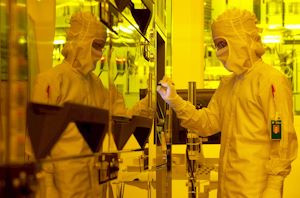
AMD Amends Wafer Supply Agreement with GlobalFoundries: 7nm Freed, 12nm+ Targets Set Through 2021
AMD on Tuesday said it had amended its wafer supply agreement with GlobalFoundries. Under the terms of the new deal, the two companies agreed about prices and volumes of...
37 by Anton Shilov on 1/29/2019
Intel Considers $11 Billion Fab in Israel
Late last year Intel announced massive plans to increase its global chip production capacities by upgrading, expanding, and equipping four of its fabs. As it turns out, the company...
37 by Anton Shilov on 1/29/2019
TSMC Chip Yields Hit By Bad Chemical Batch
TSMC on Monday said that some of the wafers it has processed recently have lower yields because of a chemical it uses during production. The company began investigation and...
28 by Anton Shilov on 1/29/2019
ASML to Ship 30 EUV Scanners in 2019: Faster EUV Tools Coming
ASML said last week that it planned to ship 30 extreme ultraviolet scanners in 2019, up significantly from 2018. The plan is not surprising, as demand for EUV lithography...
17 by Anton Shilov on 1/28/2019
ASML, Carl Zeiss, and Nikon to Settle Legal Disputes Over Immersion Lithography
Embroiled for some time now in legal disputes concerning immersion lithography, ASML, Carl Zeiss, and Nikon, this week signed a memorandum of understanding relating to a plan to once...
10 by Anton Shilov on 1/25/2019
TSMC: 7nm Now Biggest Share of Revenue
As process node technology gets ever more complex, it costs big dollars to develop and then building chips on the process is also a very costly process. The big...
44 by Ian Cutress on 1/17/2019


