Analyzing Intel-Micron 3D XPoint: The Next Generation Non-Volatile Memory
by Kristian Vättö, Ian Cutress & Ryan Smith on July 31, 2015 11:00 AM EST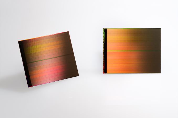
The current mainstream memory technologies, namely DRAM (quick memory accessed by the processor) and NAND (solid-state storage), have been around for decades. While the cell designs have evolved over the years to allow scaling to 20nm and below, the fundamental physics behind DRAM and NAND operation haven't changed a bit and both technologies have their unique technological limitations. DRAM offers nanosecond-level latency and unlimited endurance, but this comes at the cost of large cell size, cell volatility, and power consumption. Since DRAM cells need to be constantly refreshed, the cells don't retain data in an off state, requiring quite a bit of power and making DRAM unsuitable for permanent storage. NAND, on the other hand, has much higher latency (especially write operations) and has a limited number of write cycles, but the cells are non-volatile and the structure is much more efficient, enabling low cost and suitability for storage.
Combining DRAM and NAND at the system-level architecture provides the best of both worlds, which is why modern computers use DRAM as a memory/cache and NAND for storage. However, there's still a latency and capacity gap between DRAM and NAND, so the question arises: what if you were to combine the best of DRAM and NAND at the silicon level? The mission of next generation memory technology across the industry has been to develop a new type of memory that provides low latency and high endurance while offering a small and scalable cell size.
We have seen numerous startups, such as Crossbar and Nantero, discuss and demonstrate their next generation memory technologies, but we have yet to see the established DRAM and NAND vendors come out with their solutions. Intel and Micron are here to change that with the announcement of their new 3D XPoint (Cross Point) non-volatile memory technology this week.
First and foremost, Intel and Micron are making it clear that they are not positioning 3D XPoint as a replacement technology for either NAND or DRAM, and in that scale it has been talked about more in its applications nearer NAND than DRAM. It's supposed to complement both and provide a technology that sits in between the two by filling the latency and cost gap exists between DRAM and NAND. Basically, 3D XPoint is a new tier in the computer architecture because it can be used as either slower, non-volitile memory or much faster storage.
| DRAM | 3D XPoint | NAND | |
| Endurance (P/E Cycles) | 10^15 | 10^7 | 10^3 |
| Read Latency | Nanoseconds | 10s of Nanoseconds | ~100 Microseconds |
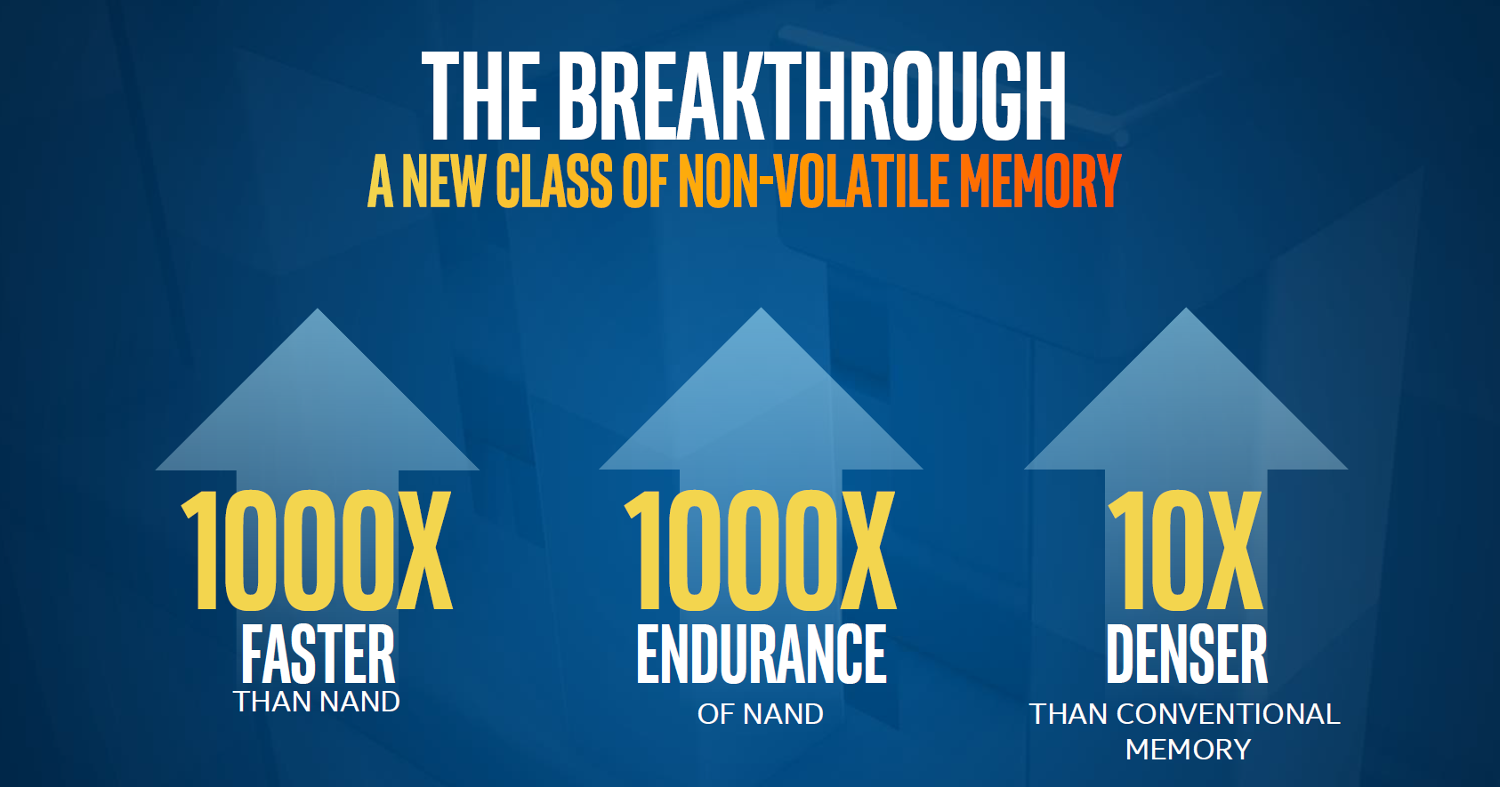
Intel and Micron are claiming that 3D XPoint provides up to a thousand times higher endurance than NAND. Assuming that the numbers are relative to modern (15-20nm) MLC NAND, the endurance should be in the order of a few million P/E cycles; though the marketing materials are claiming up to tens of millions of write cycles. If we assume 3 million write cycles (1000x of what modern MLC has), a 256GB 3D XPoint based drive would have a total write endurance of 768 petabytes. That's equivalent to 420TB per day for five years, or 4.9GB per second. For storage applications that currently rely on NAND, 3D XPoint will eliminate any potential endurance concerns, but it's not durable enough to challenge DRAM in that front since DRAM endurance is essentially infinite. Whether 3D XPoint provides enough endurance to replace DRAM ultimately depends on the application, but especially in certain enterprise workloads there's a need for DRAM.
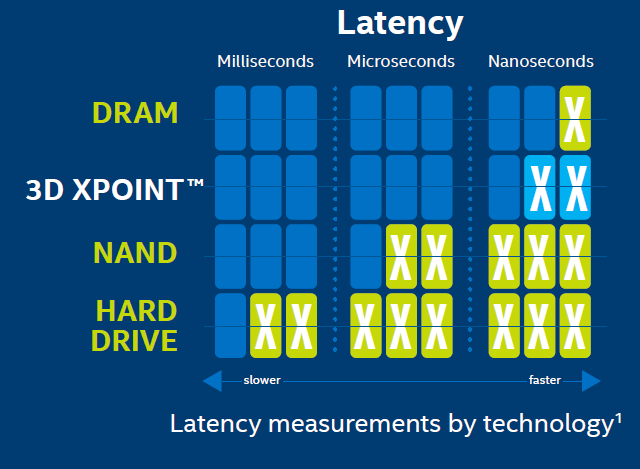
3D XPoint latency should be in the order of 10s of nanoseconds, but the companies didn't specify whether this is read or write latency. Judging by the graphs provided by Intel, it seems to be read latency because NAND write latency would measured in milliseconds (typically 1-2ms for a full page write), whereas the graph puts NAND latency at tens of microseconds that is in line with NAND read latency. Write latency is likely higher than that, probably at least 100s of nanoseconds or even a few microseconds given Intel and Micron's claims of "up to 1000x faster than NAND", but what complicates things is that 3D XPoint is accessible at the bit-level whereas NAND is page-level, so comparing the latency of the two without extended context is quite difficult. In any case, 3D XPoint performance should be closer to DRAM than NAND, but since Intel and Micron aren't discussing any specific latencies yet it's too early to make any final conclusions.
Meanwhile unlike many next generation memory technologies out there at the moment, 3D XPoint is the furthest along and doesn't only exist on paper or in a lab. Intel and Micron are currently sampling the first generation die that is being produced at the companies' jointly owned fab in Lehi, Utah. The die is 128Gbit (16GB) in capacity, whereas the products that startup memory companies have in production are in the order of dozens of megabytes. The die is built on a 20nm node and consists of two layers, and in the future scaling will happen through both lithography shrinks and by increasing the number of layers.
The Utah fab has been producing 20nm NAND for now since Intel didn't invest on the 16nm shrink and all initial 3D NAND production will take place in Micron's Singapore fab, but it's unclear whether the full fab with its 20,000 wafers per month capacity will be dedicated to 3D XPoint from now on. My guess would be that 3D XPoint will gradually take over the full wafer capacity in Utah depending on how the market reacts to the new technology and how high demand Intel and Micron are seeing. 3D XPoint does require some new equipment for manufacturing since 3D XPoint deals with a whole new set of materials, but Intel and Micron said that the transition is quite similar to a new NAND node and allows some of the existing equipment to be used.
The companies aren't quoting any price per gigabyte yet, but since the whole function of 3D XPoint is to fill the gap between DRAM and NAND, it will also be priced accordingly. A quick look at NewEgg puts DRAM pricing at approximately $5-6 per gigabyte, whereas the high-end enterprise SSDs are in the range of $2-3. While client SSDs can be had for as low as $0.35, they aren't really a fair comparison because at least initially 3D XPoint will be aimed for enterprise applications. My educated guess is that the first 3D XPoint based products will be priced at about $4 per gigabyte, possibly even slightly lower depending on how DRAM and NAND pricess fall within a year.


80 Comments
View All Comments
Alexvrb - Friday, July 31, 2015 - link
I don't think so... this is slower than current RAM. They aren't very likely to use HBM only on an APU for various reasons, so you're still going to be using something like DDR4 for your main memory. Which again, is faster than this XPoint tech.XPoint is however a lot denser than RAM, and it's non-volatile so it will make excellent high-speed storage if we can get a better interface. I think in a few years we could at least be using it as a cache for NAND devices or as "boot drives" similar to how we were using then-costly NAND-based SSDs not so long ago.
lilmoe - Monday, August 3, 2015 - link
If we're talking more in a "conventional" non-enterprise, consumer/professional product sense, then I believe this type of memory would be more of a complement to eDRAM (or other forms of higher density, lower speed cache memory), with DRAM completely omitted from the hierarchy. But this may fundamentally change the way operating systems and applications work, and depending on design/application, may lead to breakthrough performance gains.Scoobmx - Friday, July 31, 2015 - link
Ian, I have some serious doubts that this is STT-MRAM. The endurance and density numbers don't really line up. STT has virtually limitless endurance but fairly poor density due to the high current required, hence the need for a large transistor. I don't have the hubris to claim that it's impossible, but I believe it highly unlikely. Source: completed my dissertation in nanomagnetic logic and memory devices last year.J03_S - Friday, July 31, 2015 - link
It might very well be Perpendicular Magnetic Anisotropic Magnetic Tunneling Junction STT-MRAM. It's a variant of STT-MRAM that does not suffer from the density issues and is more than one order of magnitude efficient than Spin torque transfer. It was covered in the AIP journal and published back in April of 2014 by Luc Thomas and associates. At the time they had IBM producing chips for them as the entire process is fully compatible with the existing CMOS backend and requires no special changes be made to the process. This expedited the research quite a bit as they were able to test fully functioning chips.jjj - Friday, July 31, 2015 - link
About the positioning in the market you are being a bit misleading initially.The technology itsalf is likely able to compete with NAND in pricing,there would be a process and layers race but it could be doable.
So it's not really in between NAND and DRAM, cost wise, at least that's not a must, it will cost us a lot more than NAND because Intel and Micron will milk the hell out of it.
About output, that's a startegy matter, the goal being to maximize profits ,nothing else matters. The 2 companies are trying to justify their initial prices and markets by placing it inthe middle- sure it is in the middle perf wise and cost is likely higher for now than the most efficient NAND.
When you comment about power vs NAND you forget to say that it would be per bit and that's kinda relevant.
When you talk about how the laywer are made and costs, it would be important to point out that 3D NAND has very poor planar density compared to 2D NAND. the density here seems to be very close to 2D NAND density. You make it sound like it would cost a lot more than 3D NAND and don't think that's a case at all. Sure maybe it's 2-4 times more than more for now but that's not too far and it's a lot cheaper than RAM. Yes scaling the layers seems costlier here than with 3D NAND.
When talking die size it stops being as misleading as some previous bits. On die size it looks more like 18+ dies and close to 23 so some 13x16mm for 208-ish mm2.
High cell efficiency would be good too when scaling soif they go 16nm 4 layers in gen 2,it would be interesting.
Micron can double it's profits once they max that facility (and Intel takes half) , i was assuming they'll push SSDs at 4-5$ per GB too but i'm sure they'll try to go even higher if they can.
As far as i know PCI 4.0 was due in 2017 so not too far away.
You keep pushing their agenda at the end about where it can go. Look, DDR3 is some 4.5$ per GB, DDR4 getting close to 6.5$ per GB , 128Gb NAND is some 5$ but the range is pretty wide for NAND (3.5-6$). Could they sell it in phones at 1-2$ per GB? Easily, but they won't at first ,it's more profitable not to. Will they do it in gen 2-3, yeah they will. They need to expand it slowly before others have their own 3D ReRAM slutions and have a solid base by that time,whilemaking a lot of money with it in the few years of monopoly.
Ofc in phones they can go for 4-8GB at 3$ per GB and lesser RAM to save power. Don't forget power in phones, just on that and it's worth using a hybrid RAM/ReRAM in high end.
So overall i think you fail to make a clear distinction between the technology and the financial strategy. The big limitation in adoption is the very high margins, the technology itself seems plenty capable and cheap. In IoT could be interesting too when it gets cheap enough but it's not ideal since it's not quite as cheap and dense as the industry would like, a lot more is needed there long term.
Anyway, great that we have this 5 or more years before it was expected, not so great (for us) that it might take a while before prices become accessible for consumers. At least this forces others to accelerate their ReRAM roadmaps.
zodiacfml - Friday, July 31, 2015 - link
Hmm, I think I know why Intel is so invested in this. This will eventually replace NAND drives as performance storage while current NAND drives of today becomes the cold, backup storage replacing the spinning disk drives. I feel that 3D-NAND has more potential for higher density and lower power versus disks. It might become more cost effective or cheaper than hard disks when OEMs starts using NAND in cheap and mid range PCs because of the scale and less buyers of the hard disks.DrKlahn - Friday, July 31, 2015 - link
I think short term you may see Intel and Micron put a small amount of Xpoint as a read/write cache onto their Enterprise and performance oriented SSD's. It would give them a decent performance advantage with a price bump modest enough to still attract consumers.Drumsticks - Friday, July 31, 2015 - link
I've been looking forward to this writeup! I work in NSG at Intel (the Non-Volatile Memory Solutions Group i.e. the people developing 3D XPoint) and we've been super excited for this reveal.It's fun to see the industry analysis, and as always Anandtech has one of the most in-depth!
Vlad_Da_Great - Friday, July 31, 2015 - link
@Drumsticks. Keep the good work, the world is moving thanks to people like you and INTC as a company. Thank you!!!jjj - Friday, July 31, 2015 - link
Forgot to mention that in a promo video they claim SSDs with this would be up to 10x faster over PCIe/NVMe. https://www.youtube.com/watch?t=184&v=Wgk4U4qV...No idea how they do the math ofc so i wouldn't expect 10x random.