Inside OCZ's Factory: How SSDs Are Made
by Kristian Vättö on May 20, 2015 8:30 AM EST
At CES I had the opportunity to sit down with OCZ's CEO, Ralph Schmitt, to discuss the state of OCZ after Toshiba acquired the company in late 2013. We talked about how the company has changed and evolved under the new ownership and how Toshiba has brought in some much needed NAND supply and expertise. In the article we posted summarizing that discussion I also mentioned that I would be taking a closer look at OCZ's manufacturing and validation in the coming months, and today's article focuses on that.
OCZ flew me out to Taiwan to get an in-person look at the factory and I had Jason Ruppert, Senior Vice President of Operations, and Jim Van Patten, Vice President of World Wide Quality, as my hosts and guides throughout the trip, and a big thanks to both of them. A bit of background, to ensure these were the people to speak to: Mr. Ruppert has been with OCZ since March 2012 and before joining OCZ he was the Vice President of Manufacturing Operations & Engineering at Harmonic Inc, which focuses on video delivery infrastructures. Mr. Van Patten was actually Mr. Ruppert's first hire and joined the company in May 2012 from Logitech where he was the Vice President of World Wide Quality Assurance. Mr. Ruppert holds a Master's degree in Systems Engineering from North Carolina State University (for your interest, Anand did his BS in Computer Engineering in the same university), while Mr. Van Patten received his Ph.D. in Instructional Design & Evaluation from Syracuse University. It goes without saying that both Mr. Ruppert and Mr. Van Patten have extensive knowledge and experience within their operational areas, so the two were the best people to guide me through the manufacturing and validation.
The Development Process of an SSD
Before we move on to the actual factory tour and see how SSDs are made, let's outline the development process first. After all, a product must be designed and developed before it can be manufactured and there are some items that show up in both development and manufacturing processes.
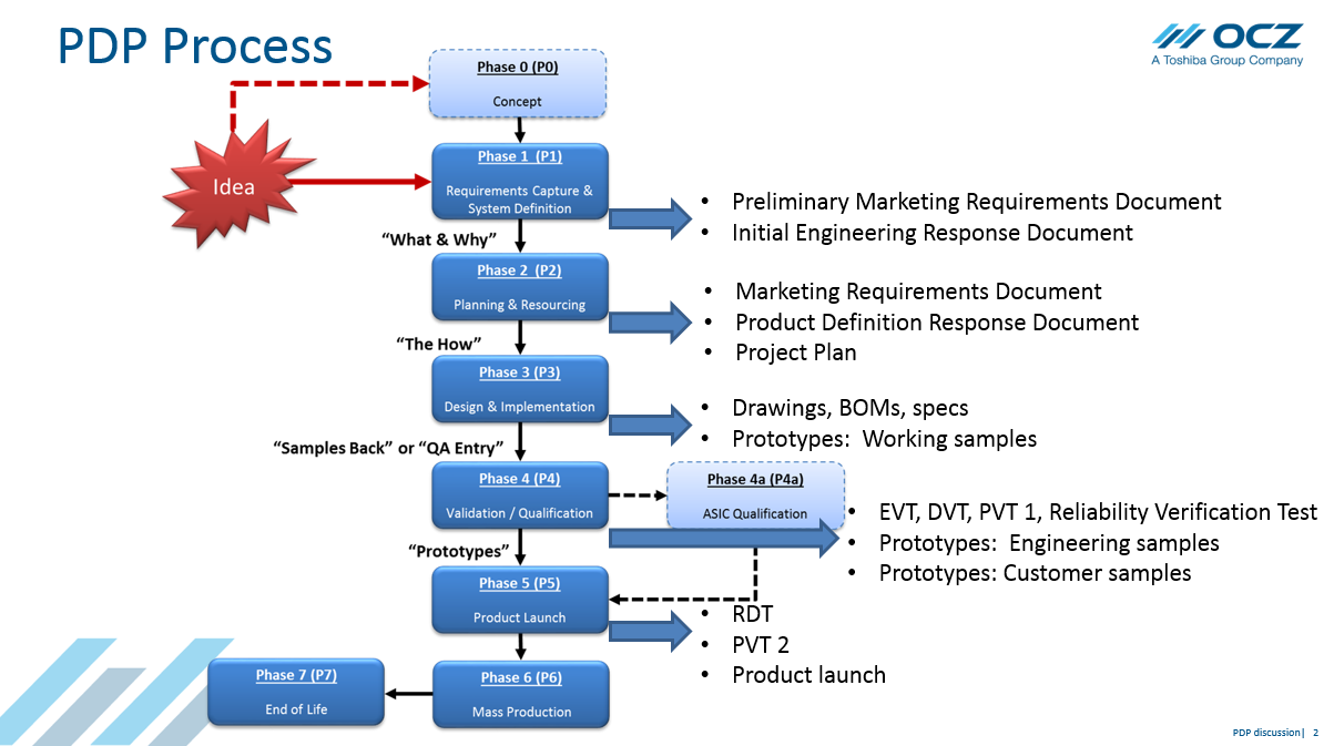
As with any product, the development process starts from an idea, which can be practically anything (completely new model, refresh of existing model with new NAND, higher capacity model, different form factor, new software etc.). In phase zero the idea is shaped to become a concept and usually results in a short (1-2 pages) document that describes the opportunity presented by the product.
Once the concept is clear, the marketing and engineering teams will give their initial feedback. Both are very important because a product must be marketable, but at the same time it needs viable to execute from the engineering standpoint. Normally phase one takes about three weeks and results in a more in-depth description of the opportunity, and if it fails at this point it is either scrapped or moved back to a concept stage.
In phase two, OCZ starts to commit more significant resources to the project. The first two phases merely outline the concept and determine its opportunity, so phase three begins the actual planning of the product. The two key documents that are finalized in this phase are the marketing requirements and engineering response documents, but each function group (e.g. quality and supply chain) will also deliver their support plans. Basically, the purpose of phase two is to construct a comprehensive project plan that includes all aspects and teams involved in the product, including the budget.
Phase two is probably the most critical phase because the project plan and budget are used to decide whether OCZ puts hundreds of thousands (or even millions) of dollars behind the product, so all documents must be carefully made and evaluated in order to make the best decision for the company. The length of phase two depends on the complexity of the product and what teams need to be involved, but it typically takes from one to three months to build the final plan and budget.
If the project is funded, OCZ moves to phase three, which is where most of the engineering work is done. OCZ of course wants to keep the exact details of this phase close to its chest, but the ultimate goal is to build the first working prototypes, so the project can move to testing the prototypes. While the engineers are busy with their work, the remaining teams work on their own functions and prepare to manufacture the pilot samples (this includes tasks such as qualifying suppliers, securing long lead time parts, developing preliminary spec sheets and marketing materials). The length of the design and implementation phase depends greatly on the product, but even a drive that uses an existing controller can spend up to a year in this phase. The development of a totally new controller like the JetExpress is obviously a multi-year project given the sheer amount of engineering work required.
The Validation Phase
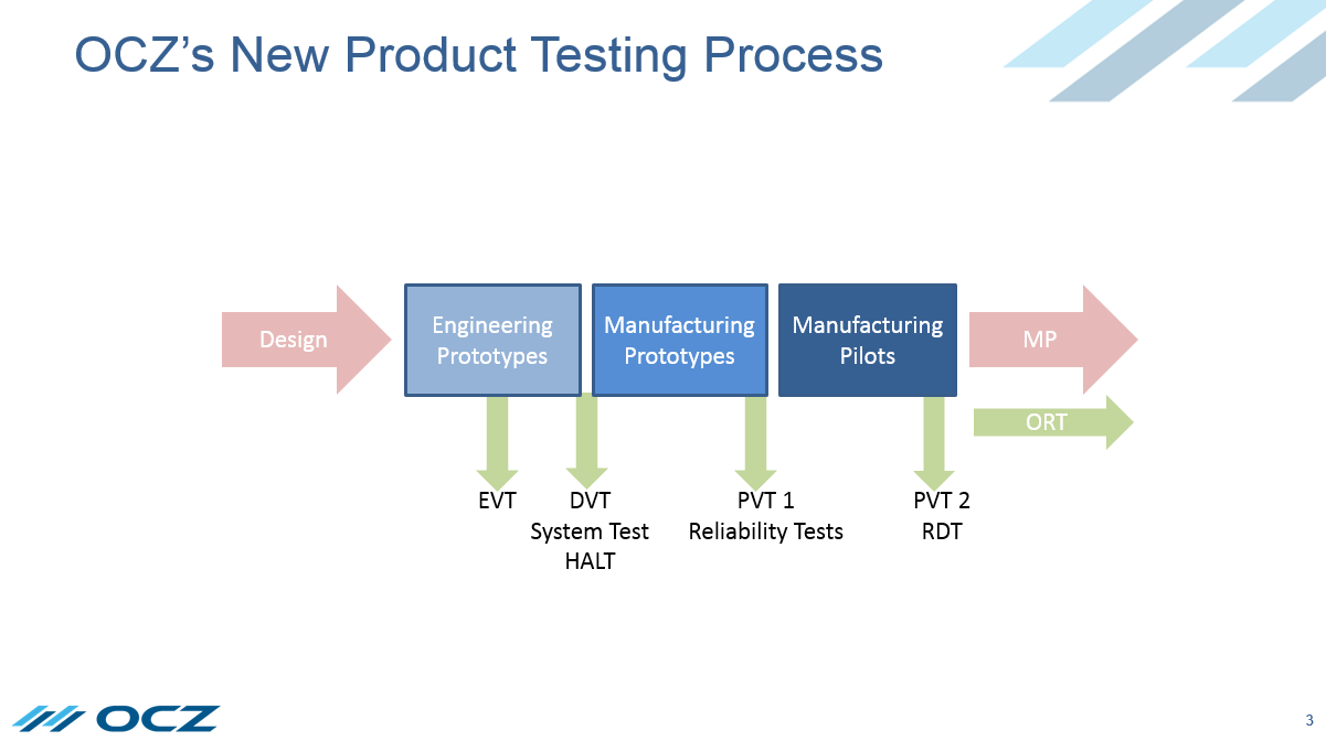
Phase four, which is validation and qualification, essentially consists of three main parts: the Engineer Verification Test (EVT), the Design Verification Test (DVT) and the Production Verification Test (PVT). EVT is run on the first engineering prototypes and it tests that the drive works in real life as it was designed to work on paper. The test suite is relatively straightforward and tests aspects such as power levels, signals and interface timings to ensure that the prototype works as it was planned to. There is also some preliminary performance testing in EVT phase, but because the firmware is usually far from final the results almost never illustrate the performance of a final product.
DVT is further broken down to two areas: normal DVT and quality/reliability. The normal DVT has a broader set of tests than EVT and more variables (e.g. power, temperature and host variations) are added to the mix to ensure that the drive operates and performs as it was supposed to in a variety of environments. Each test is also run on at least four samples, whereas the initial EVT testing is usually performed on just one or two samples. I'm not going to list and describe every individual test here because the DVT phase consists of dozens of different tests, but there are product compliance, data retention, power loss and die failure tests to mention a few, along with thorough performance testing to evaluate the firmware.
The reason why DVT is split into two parts is because EVT and normal DVT are both performed by the engineering team (who also designed the drive), which can create conflicts of interest during the validation process (in the end, human beings tend to be blind to their own faults and mistakes). Most of the DVT tests are rerun as reliability tests, but in this case the tests are performed by the independent quality team that is lead by Mr. Van Patten. The number of samples is also considerably higher and each test is run for a longer duration to verify the reliability of the design. Again, the full list of tests is several pages long, but aspects such as durability against vibration, shocks and low/high temperatures are tested in addition to the normal DVT tests. Basically every spec that is mentioned in the spec sheet is tested in this phase, including all standard JEDEC tests and certifications.
The first level of PVT tests are also run later during phase four and focus on the reliability and repeatability of the manufacturing process. Basically, the purpose of the PVT tests is to ensure that every drive coming out of the mass production line will be of the same quality and that is done by examining the drives from the production line using dye-and-pry and x-ray to inspect the PCB for any defects caused by the soldering process. The other PVT tests evaluate the readiness of the factory's quality system (incoming and in-process quality inspection, final quality control and out of box inspection) to make sure that all quality control phases are capable of separating good and bad, and that no defective products will get through to the customers. Ongoing Reliability Testing (ORT) is also set up to test a few drives from every production run to guarantee that nothing changes over time.
The total length of the validation phase varies greatly. It can be as short as two months if the design is relatively simple and similar to previous ones, but it can easily take over six months for more complex ones. Usually OCZ creates 2-5 sets of engineering samples during validation as issues are found and fixed, but there isn't really any preset duration for validation -- it always depends on what is found during the verification and how significant modifications are needed. Ultimately a drive cannot move to the next phase until it passes all quality and reliability tests, so setting a strict deadline would be a bad idea (for the company and for consumers) to begin with.
Entering Production
In phase five the drive moves from engineering and verification to operations (i.e. manufacturing), which usually takes 3-6 weeks to complete. Final PVT tests are conducted to ensure that the manufacturing quality meets the specifications and that necessary tests are in place to spot any changes/errors in the production. Other teams also finish up their actions to be ready for the launch and this is also the point when OCZ contacts us and other media about an upcoming product launch and sends out the review samples (i.e. the samples we get are typically manufacturing pilots as the mass production hasn't begun yet).
When the manufacturing side is ready to start putting out the new drive, a public announcement of the new product is made and the mass production as well as shipments to customers begin. As part of this visit, we had an inside look into the mass production side of the equation.


64 Comments
View All Comments
Pessimism - Thursday, May 21, 2015 - link
Disappointing that marketing weighs so heavily into their design process.Refuge - Thursday, May 21, 2015 - link
Thats how it is everywhere.ryanmt - Thursday, May 21, 2015 - link
"and has been achieved through science, but there's also trial and error in the mix. "What exactly to you think 'science' is?
ArmedandDangerous - Thursday, May 21, 2015 - link
Very informative, but I have to say, the writing style and quality feels like a regular blogger putting up posts on a blog. It didn't have the usual insights and technological knowledge of a Anand writer. Waiting for more works from you Kristian, and keep on improving :)Slappi - Friday, May 22, 2015 - link
Ralph Schmitt should be thrown in jail along with OCZ's former CEO who robbed shareholders of hundreds of millions of dollars. I wouldn't buy an OCZ drive if it was the fastest drive on the planet.Oxford Guy - Friday, May 22, 2015 - link
Who doesn't like a little bait and switch? Send out Vertex 2 drives with 32-bit NAND then sell drives with half the NAND chips to consumers. Whoops!Then come up with a "voluntary replacement plan" that doesn't apply to the expensive (at the time) 240 GB model. And, top it all off with spectacularly buggy drives — drives that are basically ticking time bombs waiting to brick when the user does something weird like put their laptop to sleep.
Ethos Evoss - Sunday, May 24, 2015 - link
Jeeezus picked up worst company ..Richard Buyme - Sunday, May 24, 2015 - link
Good ole' oczSame as the original ocz.safeshopper.com that conned and scammed end users when they were a reseller courtesy of Ryan Petersen
Sadly, time heals all wounds it would seem, even on the internet. Who knows how many thousands of dollars this corporation reamed out of customers' wallets back in the day (circa 2000-2001), orders taken but not shipped.
This article details some of what OCZ's founder was like before he abruptly resigned without comment in 2012
http://seekingalpha.com/instablog/890075-copperfie...
hirschma - Monday, May 25, 2015 - link
The article isn't quite correct in some areas.The first part of the process is called "stencil printing". A thin, stainless stencil is used in a stencil printer (more or less a robotic squeegee) to apply solder paste to the board. There are no sockets - the paste is applied directly to the pads.
Solder paste does not spoil after two hours; while it is temperature sensitive, it isn't that sensitive. It probably takes over two hours for a jar that size (.5 kg) to come up to room temps.
Although it isn't mentioned, I'd expect an outfit like this to do a paste inspection before the pick and place machine places the components.
Lastly, the choice of using through-hole, hand soldered SATA connectors is odd. There's no reason why they couldn't use surface mount just as easily (although through-hole is going to withstand more abuse).
hirschma - Monday, May 25, 2015 - link
Heh, took another look.If they're doing things "according to hoyle", there should be an X-Ray inspection for BTCs - bottom terminated chips. Just because a board works, doesn't mean that it'll continue to do so if there are certain defects that can only be caught that way.
Also - strangely - they do appear to be using surface mount connectors, but why they put them on in a separate process (if I read the article correctly) is very strange. Might have something to do with the testing - they may do an initial test before singulation (removing the individual boards), and then only put the connects on if it passes (the connectors are probably more expensive than the labor).
Last comment - not sure why they're using such small panels (i.e., only 4up). The standard in China is a square meter - likely due to the the contract manufacturer having equipment that can only handle smaller panels.