Intel's Sandy Bridge Architecture Exposed
by Anand Lal Shimpi on September 14, 2010 4:10 AM EST- Posted in
- CPUs
- Intel
- Sandy Bridge
A Physical Register File
Just like AMD announced in its Bobcat and Bulldozer architectures, in Sandy Bridge Intel moves to a physical register file. In Core 2 and Nehalem, every micro-op had a copy of every operand that it needed. This meant the out-of-order execution hardware (scheduler/reorder buffer/associated queues) had to be much larger as it needed to accommodate the micro-ops as well as their associated data. Back in the Core Duo days that was 80-bits of data. When Intel implemented SSE, the burden grew to 128-bits. With AVX however we now have potentially 256-bit operands associated with each instruction, and the amount that the scheduling/reordering hardware would have to grow to support the AVX execution hardware Intel wanted to enable was too much.
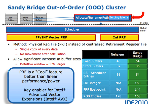
A physical register file stores micro-op operands in the register file; as the micro-op travels down the OoO engine it only carries pointers to its operands and not the data itself. This significantly reduces the power of the out of order execution hardware (moving large amounts of data around a chip eats tons of power), it also reduces die area further down the pipe. The die savings are translated into a larger out of order window.
The die area savings are key as they enable one of Sandy Bridge’s major innovations: AVX performance.
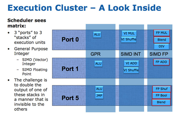
The AVX instructions support 256-bit operands, which as you can guess can eat up quite a bit of die area. The move to a physical register file enabled Intel to increase OoO buffers to properly feed a higher throughput floating point engine. Intel clearly believes in AVX as it extended all of its SIMD units to 256-bit wide. The extension is done at minimal die expense. Nehalem has three execution ports and three stacks of execution units:
Sandy Bridge allows 256-bit AVX instructions to borrow 128-bits of the integer SIMD datapath. This minimizes the impact of AVX on the execution die area while enabling twice the FP throughput, you get two 256-bit AVX operations per clock (+ one 256-bit AVX load).
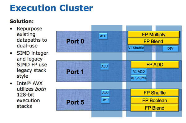
Granted you can’t mix 256-bit AVX and 128-bit integer SSE ops, however remember SNB now has larger buffers to help extract more ILP.
The upper 128-bits of the execution hardware and paths are power gated. Standard 128-bit SSE operations will not incur an additional power penalty as a result of Intel’s 256-bit expansion.
AMD sees AVX support in a different light than Intel. Bulldozer features two 128-bit SSE paths that can be combined for 256-bit AVX operations. Compared to an 8-core Bulldozer a 4-core Sandy Bridge has twice the 256-bit AVX throughput. Whether or not this is an issue going forward really depends on how well AVX is used in applications.
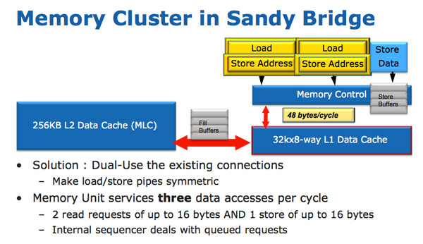
The improvements to Sandy Bridge’s FP performance increase the demands on the load/store units. In Nehalem/Westmere you had three LS ports: load, store address and store data.
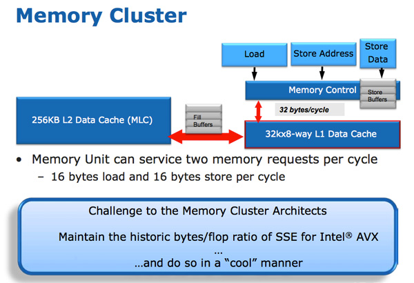
In SNB, the load and store address ports are now symmetric so each port can service a load or store address. This doubles the load bandwidth which is important as Intel doubled the peak floating point performance in Sandy Bridge.
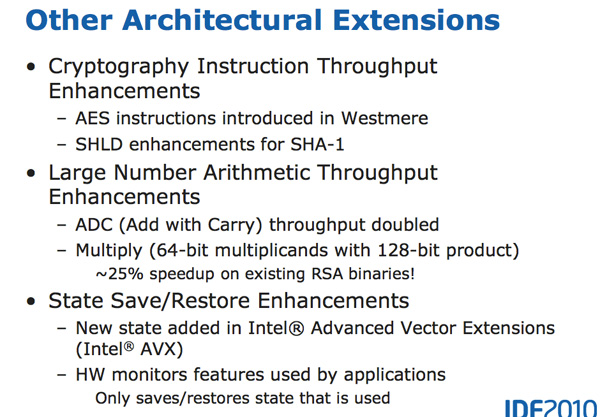
There are some integer execution improvements in Sandy Bridge, although they are more limited. Add with carry (ADC) instruction throughput is doubled, while large scale multiplies (64 * 64) see a ~25% speedup.


62 Comments
View All Comments
JoJoman88 - Wednesday, September 15, 2010 - link
To me the problem is that instead of me overclocking without reguard to TDP, now Intel will do the overclocking for me, but it will be within the TDP that Intel thinks is best. Will this not just kill the after-market cooler makers with an almost locked TDP,and to some degree high end memory maker with a locked BCLK.This will change how overclocking is done from now on unless AMD keeps things as they are and forces Intel from going down this road.
gvaley - Wednesday, September 15, 2010 - link
It's true that the CPU will turboboost within the CPU's TDP, but exactly how much it will turboboost (how much bins it will gain) will depend on how well the CPU is being chilled. So having a better (read: aftermarket) cooler will allow you to take the best of your CPU's turboboost.shodanshok - Wednesday, September 15, 2010 - link
Hi Anand,while I expect the ring bus to provide great performances, I doubt that it don't impact die size and power consumption in respect to the Nehalem/Westmere L3 organization.
Let me explain...
From my internal test, the Nehalem/Westmere L3 cache seems accessed by a four 64 bit channels (one per core). At 3 Ghz L3 cache, it translate in a maximum of 24 GB/s per core, or 96 GB/s for 4 cores. This cache organization seems confirmed by the tests at Techreport (on a i975X, SANDRA's L3 cumulative bandwidth is at about 60 GB/s: http://www.techreport.com/articles.x/18581/5) and Xbitlabs (EVEREST single-core L3 bandwidth of about 20 GB/s: http://www.xbitlabs.com/articles/cpu/display/intel...
So, on Nehalem/Westmere I do not expect 4 x 256 wires, but only 4 x 64 wires (more or less).
Now, lets examine SB...
We have 4 x 256 bit bus (4 indipendent rings) that runs around the L3 cache, for a total of 1024 wires. So, we have a lot of wires, that needs to be powered. These wires, in turn, need additional die space, and to me seems the main reason why most models will have "only" a 6 MB L3.
What do you think about? It is possible to ask Intel something about the Nehalem L3 cache organization and/or about the decision to equip most SB models with 6 MB of L3 cache?
Thanks.
Casper42 - Wednesday, September 15, 2010 - link
Knowing what you do about Nehalem EX and SNB on socket H2, any speculation on what we can expect from the Socket B2/R chips when they finally arrive sometime next year?I am mainly thinking of Northbridge/QPI and PCIe Lanes as compared to DMI used on the Mainstream parts discussed in this article.
I waited and waited for Westmere Core i7 to become "cheap" and thought the 970 was going to be my chip of choice @ $550. When they released it at $900 (you could already find 980Xs for less) it pretty much killed my plans to upgrade.
So now I am basically debating on do I build a high end H2 or wait for the enthusiast version to arrive instead?
My understanding from seeing the server roadmap is there will be Socket B2 and Socket R with the differences between them mainly consisting of memory channels and # of PCIe Lanes. I have also read that both will support PCIe 3.0 whereas H2 will continue to use 2.0.
Add all these changes up and I am also hopeful we will see USB3 on the Enthusiast platform as well since it will have an additional 3-6 months to mature.
So any ideas/insight you have here would be awesome.
linkages - Thursday, September 16, 2010 - link
With the price of LCDs dropping, I am noticing that more and more consumers have more than one display for their mainstream machines. Has Intel said anything about how many displays the onboard graphics will be able to push? Have they said anything about what tech they are going to use ie. display port, HDMI, DVI-D, something else?I can see myself getting a new SB machine sometime in Q1 2011 but I run at least 2 monitors at all times ( need the real estate for the type of work that I do ). I don't play many games but having the video decode/encode is important to me since I do tend to do some videoconferencing now a days.
The last thing I would like to know is if Intel is going to do the right thing with the drivers for their graphics. Will we humble linux users finally have a graphics driver that does not suck. Will Intel finally open source the driver so that the community can keep it updated and optimize it for X?
chukked - Thursday, September 16, 2010 - link
Hi Anand,thanks for the review, you addressed everything but left virtualization :(
which processors support vt-x and vt-d ?
iwodo - Friday, September 17, 2010 - link
x264, the best h.264 encoder there is, produce better quality video and similar speed when using "ultrafast" setting. And with 2 / 4 Core we could even transcode 2 - 4 video at the same time.The hardware encoder inside SandyBridge is not that speedy. While i could scarifies quality for speed. But Power VR's VRE Core manage 1000fps +, @ 400fps the encoder is like a waste of die space.
Intel could have further tuned the x264 for Sandy Bridge for speed and just release it with their drivers. If the hardware encoder aren't giving many times the increase in speed, then what is the point? They may as well have added extra 6 EU for GPU inside.
A Link to someone's blog posting some figures.
http://lee.hdgreetings.com/2010/09/intel-cpu-vs-nv...
Wolfpup - Wednesday, September 29, 2010 - link
Pretty disappointing. I'm sure AMD's glad though!10-30% improvement-obviously that's great, but not as big as their previous tocks if I'm remembering right, and not much different from what "ticks" like Penryn did...I know Penryn was like a 10% boost minimum over Conroe...
I'm guessing it's because they're wasting effort and die area on a worthless GPU. I *HOPE* no one on this site, no power users are going to be using that thing. (Well, okay, for a tiny notebook or something maybe...)
JumpingJack - Wednesday, September 29, 2010 - link
I don't believe you are remembering correctly.Conroe was the first tock, and certainly, it was a major leap over the P4 line. But it's bloodline was actually derived from P6, which was carried through from Banias, Dothan, then Yohna. The improvement over Yohna was in the 10-20% IPC range.
Then came Penryn the tick, which was on average only 5%, http://www.anandtech.com/show/2306/3
Then came the tock, which was Nehalem. In single threaded performance, it was roughly another 5-10% over Penryn, but in multithreaded -- again, clock for clock, it had leaps of performance, around 20-40% again. http://www.anandtech.com/show/2658/20
The tick of Nehalem was Westmere, now Westmere did not launch a quad core part so it is hard to find a clock for clock, but in single threaded performance -- roughly the same as Nehalem, factoring out any turbo advantages...
Now SB, a tick, with another 10-30% across the board both single and multithreaded, depending on workload.
Of course, the GPU is not so worthless, it is indeed challenging low end GPUs -- no doubt Llano will offer up strong GPU performance, but for the majority of the market SB is perfectly fine.
Indeed, AMD is not too happy here, at least I would suspect. On the CPU side, Intel will crush anything AMD has in the same market segement where SB resides... GPU, surely AMD will crush SB. On the CPU front, AMD is already 20-40% behind Nehalem clock for clock, core for core, SB just extends that another 10-30%.
gundersausage - Tuesday, October 26, 2010 - link
i7-950 vs i7-2500K... So which will be faster and a better gaming chip? anyone?