Intel's Sandy Bridge Architecture Exposed
by Anand Lal Shimpi on September 14, 2010 4:10 AM EST- Posted in
- CPUs
- Intel
- Sandy Bridge
A Physical Register File
Just like AMD announced in its Bobcat and Bulldozer architectures, in Sandy Bridge Intel moves to a physical register file. In Core 2 and Nehalem, every micro-op had a copy of every operand that it needed. This meant the out-of-order execution hardware (scheduler/reorder buffer/associated queues) had to be much larger as it needed to accommodate the micro-ops as well as their associated data. Back in the Core Duo days that was 80-bits of data. When Intel implemented SSE, the burden grew to 128-bits. With AVX however we now have potentially 256-bit operands associated with each instruction, and the amount that the scheduling/reordering hardware would have to grow to support the AVX execution hardware Intel wanted to enable was too much.
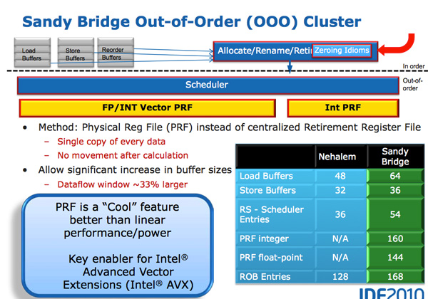
A physical register file stores micro-op operands in the register file; as the micro-op travels down the OoO engine it only carries pointers to its operands and not the data itself. This significantly reduces the power of the out of order execution hardware (moving large amounts of data around a chip eats tons of power), it also reduces die area further down the pipe. The die savings are translated into a larger out of order window.
The die area savings are key as they enable one of Sandy Bridge’s major innovations: AVX performance.
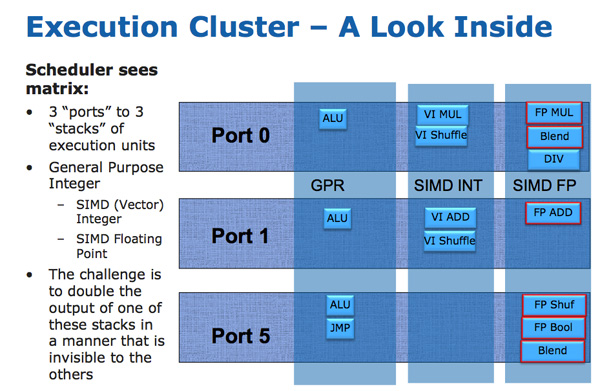
The AVX instructions support 256-bit operands, which as you can guess can eat up quite a bit of die area. The move to a physical register file enabled Intel to increase OoO buffers to properly feed a higher throughput floating point engine. Intel clearly believes in AVX as it extended all of its SIMD units to 256-bit wide. The extension is done at minimal die expense. Nehalem has three execution ports and three stacks of execution units:
Sandy Bridge allows 256-bit AVX instructions to borrow 128-bits of the integer SIMD datapath. This minimizes the impact of AVX on the execution die area while enabling twice the FP throughput, you get two 256-bit AVX operations per clock (+ one 256-bit AVX load).
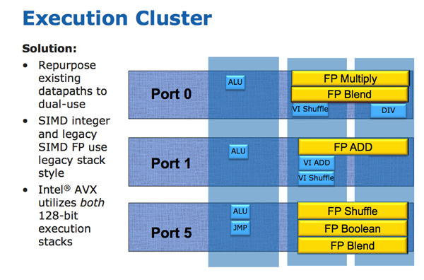
Granted you can’t mix 256-bit AVX and 128-bit integer SSE ops, however remember SNB now has larger buffers to help extract more ILP.
The upper 128-bits of the execution hardware and paths are power gated. Standard 128-bit SSE operations will not incur an additional power penalty as a result of Intel’s 256-bit expansion.
AMD sees AVX support in a different light than Intel. Bulldozer features two 128-bit SSE paths that can be combined for 256-bit AVX operations. Compared to an 8-core Bulldozer a 4-core Sandy Bridge has twice the 256-bit AVX throughput. Whether or not this is an issue going forward really depends on how well AVX is used in applications.
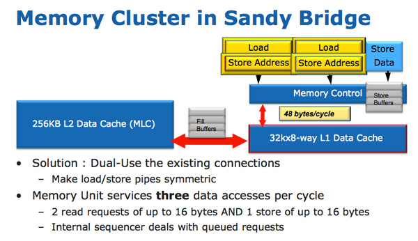
The improvements to Sandy Bridge’s FP performance increase the demands on the load/store units. In Nehalem/Westmere you had three LS ports: load, store address and store data.
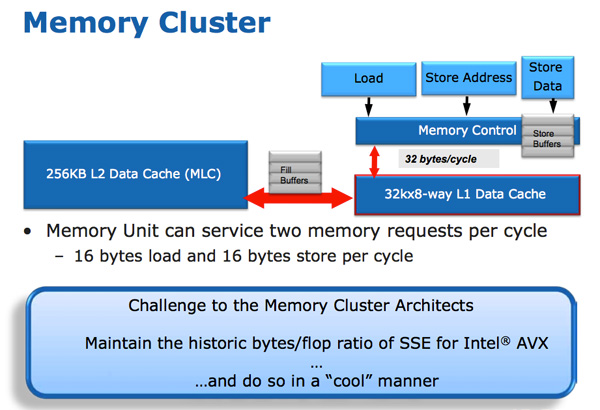
In SNB, the load and store address ports are now symmetric so each port can service a load or store address. This doubles the load bandwidth which is important as Intel doubled the peak floating point performance in Sandy Bridge.
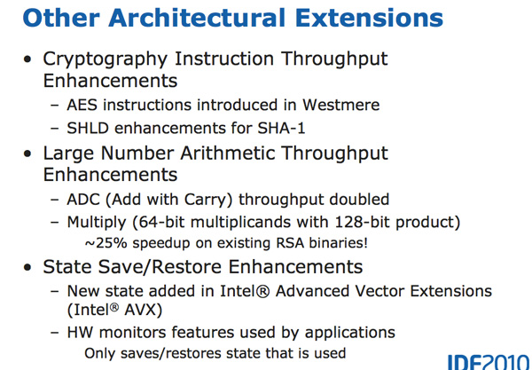
There are some integer execution improvements in Sandy Bridge, although they are more limited. Add with carry (ADC) instruction throughput is doubled, while large scale multiplies (64 * 64) see a ~25% speedup.


62 Comments
View All Comments
name99 - Tuesday, September 14, 2010 - link
This is no secret. This is exactly Intel's tick-tock strategy that has been in place for years now.The one thing you have to keep in mind is that designing these CPUs now takes of order SEVEN YEARS (!!!) from conception to ship, which means that slips and mistakes do occur. Intel (and I guess AMD) have to make their best guess as to what the market will look like in seven years and sometimes they do guess incorrectly. Of course there is scope for small changes along the way closer to the release date, but not for changes in the grand strategy.
medi01 - Tuesday, September 14, 2010 - link
Agreed, it was two things: greed and the fact that AMD is currently not in a position to be a threat.tatertot - Tuesday, September 14, 2010 - link
"The value segments won’t see Sandy Bridge until 2012."You later show a roadmap slide which indicates Sandy Bridge in the value segment in Q3 2011.
Perhaps you meant "H2 '11" instead of "2012" ?
J_Tarasovic - Thursday, September 16, 2010 - link
I think that the roadmap probably refers to OEM shipments, whereas, Anand was probably referring to when consumers would actually be able to buy devices.iwodo - Tuesday, September 14, 2010 - link
I just realize that my computer will no longer scream when i do WebCam Video Conferencing with Skype!. With the Encoder Engine and Decoder Engine, all i am doing it feeding USB 3.0 data and move them around........yuhong - Tuesday, September 14, 2010 - link
"Back in the Core Duo days that was 80-bits of data. When Intel implemented SSE, the burden grew to 128-bits. ""Core Duo" Huh?
NaN42 - Tuesday, September 14, 2010 - link
No, it seems to be right. Core Duo belongs to the Pentium M microarchitecture which implemented the SSE registers as two 64bit registers. So the largest registers were the x87-registers, but I'm not sure whether upon register renaming the registers were really copied.aka_Warlock - Tuesday, September 14, 2010 - link
New CPU from Intel... and guess what?!! New SOCKET!! Lol.Intel do know how to milk the stupid cow.
bernpi - Sunday, November 14, 2010 - link
For most people it makes perfect sense to get a new socket. Most people don't buy every new CPU from Intel or AMD because it would be a waste of money. My current CPU is a Core2Duo Quad processor with a 775 socket, i skipped the nehalem generation and will buy a SandyBridge early next year. So why should i keep my motherboard and the old 775 socket? Of course i will buy a new motherboard for the new processor. So i think for most people this is not a real issue.Sahrin - Tuesday, September 14, 2010 - link
There's a lot of "neato" stuff that does a lot to improve the user experience by making the chip use its design resources more intelligently (smarter turbo - that 'comcast turbo-boost' feature should really make a difference for end users); but in terms of actual throughput it looks like Intel left FP performance the same; and there certainly isn't any new integer hardware.K11, on the other hand, doubled integer ALU's (though the raw number of execution units is now the same as in a Nehalem core) and added a half-width (compared to Intel) FP unit.
First, I'd be interested to see if the whizz-bangies AMD was talking about for the K11 FPU a year ago make the execution time for 128-bit FP instructions comparable, better than, or still slower than Intel's FPU .
Second, I'd be quadruple interested to see what impact the way AMD is allocating the new integer hardware is going to have on performance. A monolithic Nehalem core is going to be able to handle more complex (wider) threads better than a K11 core (that's a 2-integer and 1-FPU Bulldozer); but in SMT-mode (or pseudo-SMT mode) what happens? We know Intel experiences a performance hit in HTT mode which they are only able to offset because Nehalem is so wide. AMD thinks it isn't going to get the expected hit in the front end, and they won't have the thread-switching penalty that Intel does. My prediction is that 8-core K11/Bullzoder will crush Sandy Bridge in multithreaded FP-light workloads and be 5-20% slower in everything else (the possible exception being 128-bit floats).
I'm actually kind of disappointed by this update to Nehalem...Intel did a lot of "uncore" stuff and implemenated AVX. Where's our wider back-end? More execution hardware drives better single-thread performance...the rest is just undoing the damage from the CISC-RISC transition in the front end and OoO .