Intel's Sandy Bridge Architecture Exposed
by Anand Lal Shimpi on September 14, 2010 4:10 AM EST- Posted in
- CPUs
- Intel
- Sandy Bridge
The Front End
Sandy Bridge’s CPU architecture is evolutionary from a high level viewpoint but far more revolutionary in terms of the number of transistors that have been changed since Nehalem/Westmere.
In Core 2 Intel introduced a block of logic called the Loop Stream Detector (LSD). The LSD would detect when the CPU was executing a software loop turn off the branch predictor and fetch/decode engines and feed the execution units through micro-ops cached by the LSD. This approach saves power by shutting off the front end while the loop executes and improves performance by feeding the execution units out of the LSD.
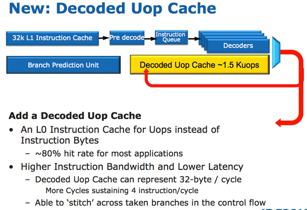
In Sandy Bridge, there’s now a micro-op cache that caches instructions as they’re decoded. There’s no sophisticated algorithm here, the cache simply grabs instructions as they’re decoded. When SB’s fetch hardware grabs a new instruction it first checks to see if the instruction is in the micro-op cache, if it is then the cache services the rest of the pipeline and the front end is powered down. The decode hardware is a very complex part of the x86 pipeline, turning it off saves a significant amount of power. While Sandy Bridge is a high end architecture, I feel that the micro-op cache would probably benefit Intel’s Atom lineup down the road as the burden of x86 decoding is definitely felt in these very low power architectures.
The cache is direct mapped and can store approximately 1.5K micro-ops, which is effectively the equivalent of a 6KB instruction cache. The micro-op cache is fully included in the L1 i-cache and enjoys approximately an 80% hit rate for most applications. You get slightly higher and more consistent bandwidth from the micro-op cache vs. the instruction cache. The actual L1 instruction and data caches haven’t changed, they’re still 32KB each (for total of 64KB L1).
All instructions that are fed out of the decoder can be cached by this engine and as I mentioned before, it’s a blind cache - all instructions are cached. Least recently used data is evicted as it runs out of space.
This may sound a lot like Pentium 4’s trace cache but with one major difference: it doesn’t cache traces. It really looks like an instruction cache that stores micro-ops instead of macro-ops (x86 instructions).
Along with the new micro-op cache, Intel also introduced a completely redesigned branch prediction unit. The new BPU is roughly the same footprint as its predecessor, but is much more accurate. The increase in accuracy is the result of three major innovations.
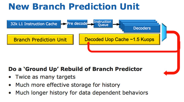
The standard branch predictor is a 2-bit predictor. Each branch is marked in a table as taken/not taken with an associated confidence (strong/weak). Intel found that nearly all of the branches predicted by this bimodal predictor have a strong confidence. In Sandy Bridge, the bimodal branch predictor uses a single confidence bit for multiple branches rather than using one confidence bit per branch. As a result, you have the same number of bits in your branch history table representing many more branches, which can lead to more accurate predictions in the future.
Branch targets also got an efficiency makeover. In previous architectures there was a single size for branch targets, however it turns out that most targets are relatively close. Rather than storing all branch targets in large structures capable of addressing far away targets, SNB now includes support for multiple branch target sizes. With smaller target sizes there’s less wasted space and now the CPU can keep track of more targets, improving prediction speed.
Finally we have the conventional method of increasing the accuracy of a branch predictor: using more history bits. Unfortunately this only works well for certain types of branches that require looking at long patterns of instructions, and not well for shorter more common branches (e.g. loops, if/else). Sandy Bridge’s BPU partitions branches into those that need a short vs. long history for accurate prediction.


62 Comments
View All Comments
name99 - Tuesday, September 14, 2010 - link
This is no secret. This is exactly Intel's tick-tock strategy that has been in place for years now.The one thing you have to keep in mind is that designing these CPUs now takes of order SEVEN YEARS (!!!) from conception to ship, which means that slips and mistakes do occur. Intel (and I guess AMD) have to make their best guess as to what the market will look like in seven years and sometimes they do guess incorrectly. Of course there is scope for small changes along the way closer to the release date, but not for changes in the grand strategy.
medi01 - Tuesday, September 14, 2010 - link
Agreed, it was two things: greed and the fact that AMD is currently not in a position to be a threat.tatertot - Tuesday, September 14, 2010 - link
"The value segments won’t see Sandy Bridge until 2012."You later show a roadmap slide which indicates Sandy Bridge in the value segment in Q3 2011.
Perhaps you meant "H2 '11" instead of "2012" ?
J_Tarasovic - Thursday, September 16, 2010 - link
I think that the roadmap probably refers to OEM shipments, whereas, Anand was probably referring to when consumers would actually be able to buy devices.iwodo - Tuesday, September 14, 2010 - link
I just realize that my computer will no longer scream when i do WebCam Video Conferencing with Skype!. With the Encoder Engine and Decoder Engine, all i am doing it feeding USB 3.0 data and move them around........yuhong - Tuesday, September 14, 2010 - link
"Back in the Core Duo days that was 80-bits of data. When Intel implemented SSE, the burden grew to 128-bits. ""Core Duo" Huh?
NaN42 - Tuesday, September 14, 2010 - link
No, it seems to be right. Core Duo belongs to the Pentium M microarchitecture which implemented the SSE registers as two 64bit registers. So the largest registers were the x87-registers, but I'm not sure whether upon register renaming the registers were really copied.aka_Warlock - Tuesday, September 14, 2010 - link
New CPU from Intel... and guess what?!! New SOCKET!! Lol.Intel do know how to milk the stupid cow.
bernpi - Sunday, November 14, 2010 - link
For most people it makes perfect sense to get a new socket. Most people don't buy every new CPU from Intel or AMD because it would be a waste of money. My current CPU is a Core2Duo Quad processor with a 775 socket, i skipped the nehalem generation and will buy a SandyBridge early next year. So why should i keep my motherboard and the old 775 socket? Of course i will buy a new motherboard for the new processor. So i think for most people this is not a real issue.Sahrin - Tuesday, September 14, 2010 - link
There's a lot of "neato" stuff that does a lot to improve the user experience by making the chip use its design resources more intelligently (smarter turbo - that 'comcast turbo-boost' feature should really make a difference for end users); but in terms of actual throughput it looks like Intel left FP performance the same; and there certainly isn't any new integer hardware.K11, on the other hand, doubled integer ALU's (though the raw number of execution units is now the same as in a Nehalem core) and added a half-width (compared to Intel) FP unit.
First, I'd be interested to see if the whizz-bangies AMD was talking about for the K11 FPU a year ago make the execution time for 128-bit FP instructions comparable, better than, or still slower than Intel's FPU .
Second, I'd be quadruple interested to see what impact the way AMD is allocating the new integer hardware is going to have on performance. A monolithic Nehalem core is going to be able to handle more complex (wider) threads better than a K11 core (that's a 2-integer and 1-FPU Bulldozer); but in SMT-mode (or pseudo-SMT mode) what happens? We know Intel experiences a performance hit in HTT mode which they are only able to offset because Nehalem is so wide. AMD thinks it isn't going to get the expected hit in the front end, and they won't have the thread-switching penalty that Intel does. My prediction is that 8-core K11/Bullzoder will crush Sandy Bridge in multithreaded FP-light workloads and be 5-20% slower in everything else (the possible exception being 128-bit floats).
I'm actually kind of disappointed by this update to Nehalem...Intel did a lot of "uncore" stuff and implemenated AVX. Where's our wider back-end? More execution hardware drives better single-thread performance...the rest is just undoing the damage from the CISC-RISC transition in the front end and OoO .