Intel's Sandy Bridge Architecture Exposed
by Anand Lal Shimpi on September 14, 2010 4:10 AM EST- Posted in
- CPUs
- Intel
- Sandy Bridge
Sandy Bridge Graphics
The largest performance improvement on Sandy Bridge vs. current Westmere architectures actually has nothing to do with the CPU, it’s all graphics. While the CPU cores show a 10 - 30% improvement in performance, Sandy Bridge graphics performance is easily double what Intel delivered with Clarkdale/Arrandale at the beginning of the year.
While the ‘dales improved performance by moving graphics to a 45nm process, increasing shader hardware and clock speed, SNB graphics improves through a significant increase in IPC.
The Sandy Bridge GPU is on-die built out of the same 32nm transistors as the CPU cores. The GPU is on its own power island and clock domain. The GPU can be powered down or clocked up independently of the CPU. Graphics turbo is available on both desktop and mobile parts, and you get more bins with graphics turbo on Sandy Bridge than you did with Arrandale.
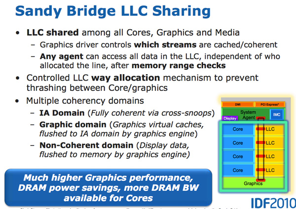
The GPU is treated like an equal citizen in the Sandy Bridge world, it gets equal access to the L3 cache. The graphics driver controls what gets into the L3 cache and you can even limit how much cache the GPU is able to use. Storing graphics data in the cache is particularly important as it saves trips to main memory which are costly from both a performance and power standpoint. Redesigning a GPU to make use of a cache isn’t a simple task. It usually requires the sort of complete re-design that NVIDIA did with GF100 for example.
SNB graphics is the anti-Larrabee. While Larrabee focused on extensive use of fully programmable hardware (with the exception of the texture hardware), SNB graphics (internally referred to as Gen 6 graphics) makes extensive use of fixed function hardware. The design mentality was anything that could be described by a fixed function should be implemented in fixed function hardware. The benefit is performance/power/die area efficiency, at the expense of flexibility. Keeping much of the GPU fixed function is in-line with Intel’s CPU centric view of the world. By contrast, taking the GPU as programmable as possible makes more sense for a GPU focused company like NVIDIA.
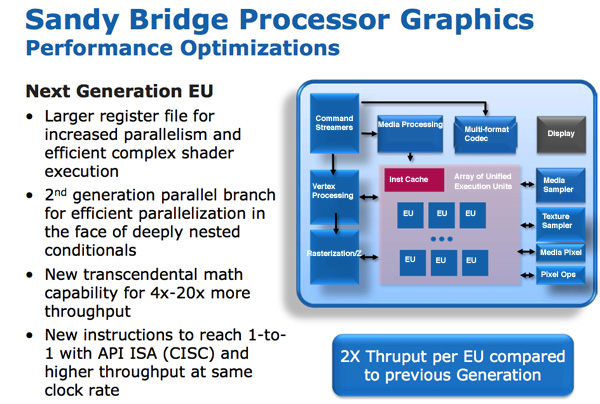
The programmable shader hardware is composed of shaders/cores/execution units that Intel calls EUs. Each EU can dual issue picking instructions from multiple threads. The internal ISA maps one-to-one with most DirectX 10 API instructions resulting in a very CISC-like architecture. Moving to one-to-one API to instruction mapping increases IPC by effectively increasing the width of the EUs.
There are other improvements within the EU. Transcendental math is handled by hardware in the EU and its performance has been sped up considerably. Intel told us that sine and cosine operations are several orders of magnitude faster now than they were in current HD Graphics.
In previous Intel graphics architectures the register file was repartitioned on the fly. If a thread needed fewer registers, the remaining registers could be allocated to another thread. While this was a great approach for saving die area, it proved to be a limiter for performance. In many cases threads couldn’t be worked on as there were no registers available for use. Prior to Intel HD Graphics each thread had an average of 64 registers, the ‘dales brought that average up to 80 per thread. In SNB, the GPU has a fixed amount of registers per thread: 120. The register count limiting thread count scenarios have been alleviated.
All of these enhancements result in 2x the instruction throughput per EU compared to Intel’s HD Graphics today.

Sandy Bridge vs. NVIDIA GeForce 310M Playing Starcraft 2
At launch there will be two versions of Sandy Bridge graphics: one with 6 EUs and one with 12 EUs. All mobile parts (at launch) will use 12 EUs, while desktop SKUs may either use 6 or 12 depending on the model. From what I’ve heard, the higher end SKUs may have 12 while the lower end models will have 6 but I haven’t seen it on a roadmap yet so I can’t confirm. With a 2x improvement in throughput per EU, you should see greater than Intel HD Graphics performance even with the 6 EU parts (thanks to higher clock speeds and the GPU sharing the L3 cache).


62 Comments
View All Comments
FXi - Tuesday, September 14, 2010 - link
Only thing I am saddened by is that hybrid graphics apparently won't be "working" on the mobile high end chipset with the dual pci-e x8 lanes. It's extremely nice to have 2x a good modern mobile GPU, but still be able to switch to the Intel built in GPU when you want longer battery life on the road.That ability, in the 2920 was something I was truly hoping for.
The rest of its abilities are quite nice and very welcome. USB 3 really is something to be sure they didn't miss. But otherwise kudos Intel.
Drazick - Tuesday, September 14, 2010 - link
Anand, few questions with your permission:I wonder If we could use a Discrete Graphics Card and enable the Media Engine.
What about the DMI bus, Hasn't it become a bottleneck with SSD Drives and USB3?
Does Intel have planes to address it?
Thanks.
EricZBA - Tuesday, September 14, 2010 - link
Someone please release a decent 13.3 inch laptop using Sandy Bridge please.bitcrazed - Tuesday, September 14, 2010 - link
I have a sneaking suspicion that Intel will be at the core of Apple's next laptop platform refresh with both SandyBridge and LightPeak.Apple's MacBook lineup is starting to feel a little pressure from the other PC laptop vendors who are starting to produce some nicely designed tin and will need to stay current in order to continue to sell their products at such high premiums.
I'm imagining the next MacBook Pro lineup to offer 13" MBP's running i3 2120's and the 15" and 17" models running i5 2400/2500's or i7 2600's.
Apple already have their own dynamic integrated/discrete GPU switching technology (as do nVidia) and can make even better use of SB's integrated GPU augmented by a modest discrete GPU to deliver the performance that most users need but with much reduced power drain.
So how to differentiate themselves? LightPeak. Apple was the instigator of LightPeak to start with and Intel claimed at CES 2010 that it'd appear around a year later. That's next spring.
One thing's for sure: 2011 is going to be a VERY interesting year for new laptop and desktop devices :)
name99 - Tuesday, September 14, 2010 - link
LightPeak WITHOUT USB3 will go over like a lead zeppelin.There are already plenty of USB3 peripherals available. I have never in my life seen a LightPeak peripheral, or even a review or sneak peek of one. Light Peak is coming, but I'm not sure that 2011 is its year.
The rate at which CPU speeds now increases is low enough that very few buyers feel any sort of pressure to upgrade the machine they bough 3 years ago. Apple can't deal with that by simply offering new iMacs and MacBooks with the newest Intel offering, since no normal person is much excited by another 10% CPU boost.
They have done an adequate job of dealing with this so far by boosting battery life, something (some) portable users do care about.
They have done a mixed job of making more cores, hyperthreading and better GPUs a reason to upgrade. We have some low-level infrastructure in Snow Leopard, but we have fsckall user level apps that take advantage of this. Where is the multi-threaded Safari? Where is the iTunes that utilizes multiple cores, and the GPU for transcoding audio? Does FileVault use AES-NI --- apparently not.
But Apple has done an truly astonishingly lousy job of tracking the one remaining piece of obvious slowness --- IO. Still no TRIM, still no eSATA, still no USB3.
My point is that I don't know the Apple politics, but I do know that they are doing a very very bad job of shipping machines that compel one to upgrade. There is no need for me to upgrade my 3+yr old Penryn iMac, for example --- I'd get a replacement with more cores (not used by any of my software), a better GPU (but what I have plays video just fine), and most importantly, NO FASTER IO.
Adding LightPeak to this mix without USB3 is not going to help any. People are still going to hold off on upgrades until USB3 is available, and no-one is going to rush to buy a LightPeak system so that they can then NOT run any of the many unavailable LightPeak peripherals on the shelves at Fry's.
NaN42 - Tuesday, September 14, 2010 - link
On page 3: "Compared to an 8-core Bulldozer a 4-core Sandy Bridge has twice the 256-bit AVX throughput."WTF? 8*128 = 4*256. Based on the premise that the fp-scheduler of one Bulldozer module (two cores) can schedule e.g. one add and one mul avx-instruction per clock cycle, they have the same throughput. I think both architectures will have a delay for e.g. shuffling ymm-registers (compared to current xmm-instructions) because data has to be exchanged between different pipelines/ports (Hopefully the picture provided by Intel is correct). Perhaps the delay is smaller in Sandy Bridge cores. I expect some delays when one mixes floating-point and integer instructions on Sandy Bridge. (Currently I don't know, whether there exists a VEX prefix for xmm integer instructions. If there's no VEX prefix the delays will be great on both platforms.)
gvaley - Tuesday, September 14, 2010 - link
"...you get two 256-bit AVX operations per clock.""AMD sees AVX support in a different light than Intel. Bulldozer features two 128-bit SSE paths that can be combined for 256-bit AVX operations. "
So it's actually 8*256 = 4*2*256. At least this is how I see it.
NaN42 - Tuesday, September 14, 2010 - link
"So it's actually 8*256 = 4*2*256. At least this is how I see it. "Ok, my calculation was a bit different. 4*2*256 will be true, but only if you mix additions and multiplications. Whether AMD is 8*2*128 depends on the fp-scheduler (based on the premise that one SIMD unit consists of a fmul, fadd and fmisc unit or something similar)
NaN42 - Tuesday, September 14, 2010 - link
... one can do another floating point operation which goes through port 5, but the peak performance of additions and multiplications is more relevant in applications.Spacksack - Tuesday, September 14, 2010 - link
I think you are right. I would think bulldozer can manage the same theoreticakl throughput by issuing one combined FMA instruction (16 flop) / clock and module.More importantly Bulldozer will achieve hight throughput for all the existing SSE code by having two independent FMA units. I have no idea how Anand could make such a mistake.