The Sandy Bridge Preview
by Anand Lal Shimpi on August 27, 2010 2:38 PM ESTA New Architecture
This is a first. Usually when we go into these performance previews we’re aware of the architecture we’re reviewing, all we’re missing are the intimate details of how well it performs. This was the case for Conroe, Nehalem and Lynnfield (we sat Westmere out until final hardware was ready). Sandy Bridge, is a different story entirely.
Here’s what we do know.
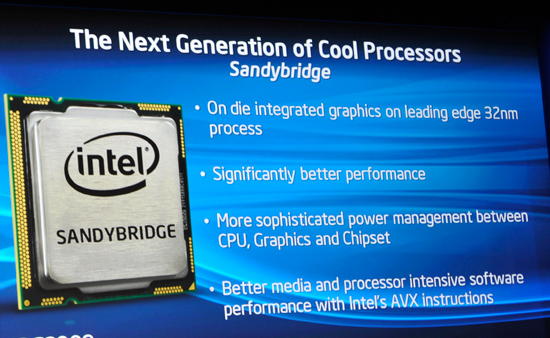
Sandy Bridge is a 32nm CPU with an on-die GPU. While Clarkdale/Arrandale have a 45nm GPU on package, Sandy Bridge moves the GPU transistors on die. Not only is the GPU on die but it shares the L3 cache of the CPU.
There are two different GPU configurations, referred to internally as 1 core or 2 cores. A single GPU core in this case refers to 6 EUs, Intel’s graphics processor equivalent (NVIDIA would call them CUDA cores). Sandy Bridge will be offered in configurations with 6 or 12 EUs.
While the numbers may not sound like much, the Sandy Bridge GPU is significantly redesigned compared to what’s out currently. Intel already announced a ~2x performance improvement compared to Clarkdale/Arrandale, and I can say that after testing Sandy Bridge Intel has been able to achieve at least that.
Both the CPU and GPU on SB will be able to turbo independently of one another. If you’re playing a game that uses more GPU than CPU, the CPU may run at stock speed (or lower) and the GPU can use the additional thermal headroom to clock up. The same applies in reverse if you’re running something computationally intensive.
On the CPU side little is known about the execution pipeline. Sandy Bridge enables support for AVX instructions, just like Bulldozer. The CPU will also have dedicated hardware video transcoding hardware to fend off advances by GPUs in the transcoding space.
Caches remain mostly unchanged. The L1 cache is still 64KB (32KB instruction + 32KB data) and the L2 is still a low latency 256KB. I measured both as still 4 and 10 cycles respectively. The L3 cache has changed however.
Only the Core i7 2600 has an 8MB L3 cache, the 2400, 2500 and 2600 have a 6MB L3 and the 2100 has a 3MB L3. The L3 size should matter more with Sandy Bridge due to the fact that it’s shared by the GPU in those cases where the integrated graphics is active. I am a bit puzzled why Intel strayed from the steadfast 2MB L3 per core Nehalem’s lead architect wanted to commit to. I guess I’ll find out more from him at IDF :)
The other change appears to either be L3 cache latency or prefetcher aggressiveness, or both. Although most third party tools don’t accurately measure L3 latency they can usually give you a rough idea of latency changes between similar architectures. In this case I turned to cachemem which reported Sandy Bridge’s L3 latency as 26 cycles, down from ~35 in Lynnfield (Lynnfield’s actual L3 latency is 42 clocks).
As I mentioned before, I’m not sure whether this is the result of a lower latency L3 cache or more aggressive prefetchers, or both. I had limited time with the system and was unfortunately unable to do much more.
And that’s about it. I can fit everything I know about Sandy Bridge onto a single page and even then it’s not telling us much. We’ll certainly find out more at IDF next month. What I will say is this: Sandy Bridge is not a minor update. As you’ll soon see, the performance improvements the CPU will offer across the board will make most anyone want to upgrade.


200 Comments
View All Comments
starx5 - Tuesday, September 7, 2010 - link
And why didn't you ran 2560x1600(or higher resolution like eyefinity) benchmark either?Is this because sandybrige is not that good?
wut - Friday, September 10, 2010 - link
So you're expecting eyeinfinity out of a single integrated graphics connection out the back of a motherboard?Are you okay?
gundersausage - Tuesday, October 26, 2010 - link
i7-950 vs i7-2500K... So which will be faster and a better gaming chip? anyone?WillyMcNilly - Thursday, October 28, 2010 - link
Fantastic preview! I am definetly getting sandy bridge now. Apparently the Gigabyte P67-UD7 will have a geforce n200 chipset and support full 16X/16X sli AND crossfire! It will make a significant upgrade from my Phenom 2 and I cannot see myself waiting for bulldozer which has apparently been delayed (gee what a surprise!) until Q4 2011.Chrisch - Wednesday, November 24, 2010 - link
which sample did you use for your tests?QDF Q12W = GT1 (850-1100MHz)
QDF Q12X = GT2 (850-1100MHz)
techeadtrevor - Thursday, December 30, 2010 - link
Hey guys, checkout this review of the i7-2600k... I think its bogus...tell me what you think of it on here.( http://en.inpai.com.cn/doc/enshowcont.asp?id=7944 )
psiboy - Sunday, January 2, 2011 - link
Catalyst 8.12... WTF! 2 year old drivers? How much did intel bribe you to use drivers that old for their competition? That is a really bad path to guy down... Tom's did weird stuff like that a while back and lost readers because of it.... You just lost my respect Anand....kmidm - Thursday, January 6, 2011 - link
I don't think an entire product line of CPU's with on-board graphics is anything really to get excited about, especially for us geeks. I guess I'm just old-school. The Sandy Bridge ,like Clarksdale, has similar benefits from a single-chip chipset which is very appealing from a throughput and control standpoint.katleo123 - Tuesday, February 1, 2011 - link
Take nother look at Sandy bridgevisit http://www.techreign.com/2010/12/intels-sandy-brid...
hapeid - Friday, March 10, 2017 - link
Wow Intel owns when it came to converting video, beating out much faster dedicated solutions, which was strange but still awesome.I don't know how AMD's going to fare but i hope their new architecture will at least compete with these CPU's, because for a few years now AMD has been at least a generation worth of speed behind Intel.
Also Intel's IGP's are finally gaining some ground in the games department.