The Sandy Bridge Preview
by Anand Lal Shimpi on August 27, 2010 2:38 PM ESTA New Architecture
This is a first. Usually when we go into these performance previews we’re aware of the architecture we’re reviewing, all we’re missing are the intimate details of how well it performs. This was the case for Conroe, Nehalem and Lynnfield (we sat Westmere out until final hardware was ready). Sandy Bridge, is a different story entirely.
Here’s what we do know.
Sandy Bridge is a 32nm CPU with an on-die GPU. While Clarkdale/Arrandale have a 45nm GPU on package, Sandy Bridge moves the GPU transistors on die. Not only is the GPU on die but it shares the L3 cache of the CPU.
There are two different GPU configurations, referred to internally as 1 core or 2 cores. A single GPU core in this case refers to 6 EUs, Intel’s graphics processor equivalent (NVIDIA would call them CUDA cores). Sandy Bridge will be offered in configurations with 6 or 12 EUs.
While the numbers may not sound like much, the Sandy Bridge GPU is significantly redesigned compared to what’s out currently. Intel already announced a ~2x performance improvement compared to Clarkdale/Arrandale, and I can say that after testing Sandy Bridge Intel has been able to achieve at least that.
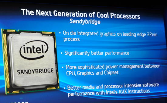
Both the CPU and GPU on SB will be able to turbo independently of one another. If you’re playing a game that uses more GPU than CPU, the CPU may run at stock speed (or lower) and the GPU can use the additional thermal headroom to clock up. The same applies in reverse if you’re running something computationally intensive.
On the CPU side little is known about the execution pipeline. Sandy Bridge enables support for AVX instructions, just like Bulldozer. The CPU will also have dedicated hardware video transcoding hardware to fend off advances by GPUs in the transcoding space.
Caches remain mostly unchanged. The L1 cache is still 64KB (32KB instruction + 32KB data) and the L2 is still a low latency 256KB. I measured both as still 4 and 10 cycles respectively. The L3 cache has changed however.
Only the Core i7 2600 has an 8MB L3 cache, the 2400, 2500 and 2600 have a 6MB L3 and the 2100 has a 3MB L3. The L3 size should matter more with Sandy Bridge due to the fact that it’s shared by the GPU in those cases where the integrated graphics is active. I am a bit puzzled why Intel strayed from the steadfast 2MB L3 per core Nehalem’s lead architect wanted to commit to. I guess I’ll find out more from him at IDF :)
The other change appears to either be L3 cache latency or prefetcher aggressiveness, or both. Although most third party tools don’t accurately measure L3 latency they can usually give you a rough idea of latency changes between similar architectures. In this case I turned to cachemem which reported Sandy Bridge’s L3 latency as 26 cycles, down from ~35 in Lynnfield (Lynnfield’s actual L3 latency is 42 clocks).
As I mentioned before, I’m not sure whether this is the result of a lower latency L3 cache or more aggressive prefetchers, or both. I had limited time with the system and was unfortunately unable to do much more.
And that’s about it. I can fit everything I know about Sandy Bridge onto a single page and even then it’s not telling us much. We’ll certainly find out more at IDF next month. What I will say is this: Sandy Bridge is not a minor update. As you’ll soon see, the performance improvements the CPU will offer across the board will make most anyone want to upgrade.


200 Comments
View All Comments
seapeople - Sunday, August 29, 2010 - link
So you're saying that integrated graphics should either be able to handle high resolution gaming using at least medium settings on the upper echelon of current games or they should not be included? That's fairly narrow minded. The bottom line is that most people will never need a better graphics card than SB provides, and the people who do are probably going to buy a $200+ graphics card anyway and replace it every summer, so are they really going to care if the integrated graphics drive the price of their $200 processor up by $10-20? Alternatively, this chip is begging for some sort of Optimus-like option, which will allow hardcore gamers to buy the graphics card they want, AND not have to chew up 100W of graphics power while browsing the web or watching a movie.Regardless, for people who aren't hard core gamers, the IGP on SB replaces the need to buy something like a Radeon HD 5450, ultimately saving them money. This seems like a positive step to me.
chizow - Sunday, August 29, 2010 - link
No, I'm saying if this is being advertised as a suitable discrete GPU replacement, it should be compared to discrete GPUs at resolutions and settings you would expect a discrete GPU to handle and not IGPs that we already know are too slow to matter. 1024x768 and all lowest settings doesn't fit that criteria. Flash and web-based games don't either, since they don't even require a 3D accelerator in order to run (Intel's workaround Broadcom chip would be fine).Again, this card wouldn't even hold a candle to a mid-range $200 GPU from 3 years ago, the 8800GT would still do cartwheels all over it. You can buy these cards for much less than $100, even the GT240 or 4850 for example have been selling for less than $50 after MIR and would be a much more capable gaming card.
Also, you're badly mistaken if you think this GPU is free by any means, as the cost to integrate a GPU onto SB's die comes at the expense of what could've been more actual CPU....so instead of better CPU performance this generation, you lose that for mediocre graphics performance. There is a price to pay for that relatively massive IGP whether you think so or not, you are paying for it.
wut - Sunday, August 29, 2010 - link
You don't know what you're talking about. You pretend that you do, but you don't.The telling sign is your comment about L2/L3 cache.
chizow - Sunday, August 29, 2010 - link
Actually it sounds like you don't know what you're talking about or you didn't read the article:"Only the Core i7 2600 has an 8MB L3 cache, the 2400, 2500 and 2600 have a 6MB L3 and the 2100 has a 3MB L3. The L3 size should matter more with Sandy Bridge due to the fact that it’s shared by the GPU in those cases where the integrated graphics is active. I am a bit puzzled why Intel strayed from the steadfast 2MB L3 per core Nehalem’s lead architect wanted to commit to. I guess I’ll find out more from him at IDF :)"
You might've missed it very clearly stated in the tables also that only the 2600 has the same 8MB L3 or 2MB per core with previous 4C like Bloomfield/Lynnfield/Westmere/Clarkdale. The rest have 6MB or 3MB, which is less than 8MB or 4MB L3 used on the previous generation chips.
This may change with the high-end/enthusiast platform, but again, the amount of L3 cache is actually going to be a downgrade on many of these Sandy Bridge SKUs for anyone who already owns a Nehalem/Westmere based CPU.
wut - Friday, September 10, 2010 - link
You're parroting Anand and his purely number-based guess. Stop pretending.mac2j - Saturday, August 28, 2010 - link
990x is a Gulftown part on 1366 that's 130MHz faster than the 980x.... will cost $1000 and come out the same time as the 2600 (which will cost ~ 1/2 and deliver 90% of the performance) and at most a couple months before the i7-2800K which will cost less and trounce it performance-wise.You'd have to REALLY want those extra cores to buy a 990x on a lame-duck socket at that point!
wut - Sunday, August 29, 2010 - link
Some has to get those chips to populate the uppermost echelons 3DMark score boards. It's an expensive hobby.hybrid2d4x4 - Saturday, August 28, 2010 - link
Anand, can you provide some more info on what the system configuration was when running the power tests? The test setup lists 2 vid cards and it's not clear which was used when deriving the power graphs. Also, what PSU was used?Just wondering since if it was a 1200W behemoth, then the 63W idle might really be 30W on a more reasonable PSU (assuming no vid cards)...
As always, thanks for the article!
smilingcrow - Saturday, August 28, 2010 - link
Was HT enabled for the power tests and what application was used to load the cores?semo - Saturday, August 28, 2010 - link
No USB3.0 support and a half baked SATA3 implementation. I could be a bit too harsh about the latter (can't say if SATA3 on a 6 series chipset will perform poorly or not) but why are they going with only 2 6Gb/s ports? I understand that most people are likely to be buying only 1 or so SSDs in the near future but what about in a few years when these things become mainstream? At least AMD took SATA3 seriously even if they couldn't quite make it work initially (we need a follow up on the 8 series chipsets' SATA performance!)Not only are Intel overlooking advance in technologies other than CPUs (which are important to most consumers, whether they are aware of it or not) but are also denying other companies who might have more focus in those areas. I wonder if Nvidia or someone else bother to release a chipset for Intel's latest and greatest.