The Sandy Bridge Preview
by Anand Lal Shimpi on August 27, 2010 2:38 PM ESTUpdate: Be sure to read our Sandy Bridge Architecture Exposed article for more details on the design behind Intel's next-generation microprocessor architecture.
The mainstream quad-core market has been neglected ever since we got Lynnfield in 2009. Both the high end and low end markets saw a move to 32nm, but if you wanted a mainstream quad-core desktop processor the best you could get was a 45nm Lynnfield from Intel. Even quad-core Xeons got the 32nm treatment.
That's all going to change starting next year. This time it's the masses that get the upgrade first. While Nehalem launched with expensive motherboards and expensive processors, the next tock in Intel's architecture cadence is aimed right at the middle of the market. This time, the ultra high end users will have to wait - if you want affordable quad-core, if you want the successor to Lynnfield, Sandy Bridge is it.
Sandy Bridge is the next major architecture from Intel. What Intel likes to call a tock. The first tock was Conroe, then Nehalem and now SB. In between were the ticks - Penryn, Westmere and after SB we'll have Ivy Bridge, a 22nm shrink of Sandy.
Did I mention we have one?
While Intel is still a few weeks away from releasing Sandy Bridge performance numbers at IDF, we managed to spend some time with a very healthy sample and run it through a few of our tests to get a sneak peak at what's coming in Q1 2011.
New Naming
The naming isn’t great. It’s an extension of what we have today. Intel is calling Sandy Bridge the 2nd generation Core i7, i5 and i3 processors. As a result, all of the model numbers have a 2 preceding them.
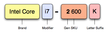
For example, today the fastest LGA-1156 processor is the Core i7 880. When Sandy Bridge launches early next year, the fastest LGA-1155 processor will be the Core i7 2600. The two indicates that it’s a 2nd generation Core i7, and the 600 is the model number.
| Sandy Bridge CPU Comparison | |||||||||
| Base Frequency | L3 Cache | Cores/Threads | Max Single Core Turbo | Intel HD Graphics Frequency/Max Turbo | Unlocked | TDP | |||
| Intel Core i7 2600K | 3.4GHz | 8MB | 4 / 8 | 3.8GHz | 850 / 1350MHz | Y | 95W | ||
| Intel Core i7 2600 | 3.4GHz | 8MB | 4 / 8 | 3.8GHz | 850 / 1350MHz | N | 95W | ||
| Intel Core i5 2500K | 3.3GHz | 6MB | 4 / 4 | 3.7GHz | 850 / 1100MHz | Y | 95W | ||
| Intel Core i5 2500 | 3.3GHz | 6MB | 4 / 4 | 3.7GHz | 850 / 1100MHz | N | 95W | ||
| Intel Core i5 2400 | 3.1GHz | 6MB | 4 / 4 | 3.4GHz | 850 / 1100MHz | N | 95W | ||
| Intel Core i3 2120 | 3.3GHz | 3MB | 2 / 4 | N/A | 850 / 1100MHz | N | 65W | ||
| Intel Core i3 2100 | 3.1GHz | 3MB | 2 / 4 | N/A | 850 / 1100MHz | N | 65W | ||
The names can also have a letter after four digit model number. You’re already familiar with one: K denotes an unlocked SKU (similar to what we have today). There are two more: S and T. The S processors are performance optimized lifestyle SKUs, while the T are power optimized.
The S parts run at lower base frequencies than the non-S parts (e.g. a Core i7 2600 runs at 3.40GHz while a Core i7 2600S runs at 2.80GHz), however the max turbo frequency is the same for both (3.8GHz). GPU clocks remain the same but I’m not sure if they have the same number of execution units. All of the S parts run at 65W while the non-S parts are spec’d at 95W.
| Sandy Bridge CPU Comparison | ||||||||
| Base Frequency | L3 Cache | Cores/Threads | Max Single Core Turbo | Intel HD Graphics Frequency/Max Turbo | TDP | |||
| Intel Core i7 2600S | 2.8GHz | 8MB | 4 / 8 | 3.8GHz | 850 / 1100MHz | 65W | ||
| Intel Core i5 2500S | 2.7GHz | 6MB | 4 / 4 | 3.7GHz | 850 / 1100MHz | 65W | ||
| Intel Core i5 2500T | 2.3GHz | 6MB | 4 / 4 | 3.3GHz | 650 / 1250MHz | 45W | ||
| Intel Core i5 2400S | 2.5GHz | 6MB | 4 / 4 | 3.3GHz | 850 / 1100MHz | 65W | ||
| Intel Core i5 2390T | 2.7GHz | 3MB | 2 / 4 | 3.5GHz | 650 / 1100MHz | 35W | ||
| Intel Core i3 2100T | 2.5GHz | 3MB | 2 / 4 | N/A | 650 / 1100MHz | 35W | ||
The T parts run at even lower base frequencies and have lower max turbo frequencies. As a result, these parts have even lower TDPs (35W and 45W).
I suspect the S and T SKUs will be mostly used by OEMs to keep power down. Despite the confusion, I like the flexibility here. Presumably there will be a price premium for these lower wattage parts.


200 Comments
View All Comments
overzealot - Saturday, August 28, 2010 - link
Now, that's a name I've not heard in a long time. A long time.mapesdhs - Saturday, August 28, 2010 - link
Seems to be Intel is slowly locking up the overclocking scene because it has no
competition. If so, and Intel continues in that direction, then it would be a great
chance for AMD to win back overclocking fans with something that just isn't
locked out in the same way.
Looking at the performance numbers, I see nothing which suggests a product that
would beat my current 4GHz i7 860, except for the expensive top-end unlocked
option which I wouldn't consider anyway given the price.
Oh well, perhaps my next system will be a 6-core AMD.
Ian.
LuckyKnight - Saturday, August 28, 2010 - link
Do we have something more precise about the release date? Q1 is what - Jan/Feb/March/Apri?Looking to upgrade a core 2 duo at the moment - not sure whether to wait
mino - Saturday, August 28, 2010 - link
Q1 (in this case) means tricle amounts in Jan/Feb, mainstream availability Mar/April and worth-buying mature mobos in May/June timeframe.tatertot - Saturday, August 28, 2010 - link
Intel has already announced that shipments for revenue will occur in Q4 of this year. So, January launch.They've also commented that Sandy Bridge OEM demand is very strong, and they are adjusting the 32nm ramp up to increase supply. So January should be a decent launch.
Not surprising-- these parts have been in silicon since LAST summer.
chrsjav - Saturday, August 28, 2010 - link
Do modern clock generators use a quartz resonator? How would that be put on-die?iwodo - Saturday, August 28, 2010 - link
Since you didn't get this chip directly from Intel , i suspect there were no reviews guideline for you to follow, like which test to run and what test not to run etc.Therefore those benchmark from Games were not a results of special optimization in drivers. Which is great, because drivers matter much more then Hardware in GPU. If these are only early indication of what Intel new GPU can do, i expect there are more to extract from drivers.
You mention 2 Core GPU ( 12 EU ) verus 1 GPU ( 6 EU ), Any Guess as to what "E" stand for? And it seems like a SLI like tech rather then actually having more EU in one chip. The different being SLI or crossfire does not get any advantage unless drivers and games are working together. Which greatly reduces the chances of it working at full performance.
It also seems every one fail to realize one of the greatest performance will be coming from AVX. AVX will be like MMX again when we had the Pentium. I cant think of any other SSE having as great important to performance as AVX. Once software are specially optimize for AVX we should get another major lift in performance.
I also heard about rumors that 64bit in Sandy Bridge will work much better. But i dont know if there are anything we could test this.
The OpenCL sounds like a Intel management decision rather then a technical decision. May be Intel will provide or work with Apple to provide OpenCL on these GPU?
You also mention that Intel somehow support PCI -Express 2.0 with 1.0 performance. I dont get that bit there. Could you elaborate? 2.5GT/s for G45 Chipset??
If Intel ever decide to finally work on their drivers, then their GPU will be great for entry levels.
Are Dual Channel DDR3 1333 enough for Quad Core CPU + GPU? or even Dual core CPU.
Is GPU memory bandwidth limited?
Any update on Hardware Decoder? And what about transcoding part?
Would there be ways to lock the GPU to run at Turbo Clock all the time? Or GPU gets higher priority in Turbo etc..
How big is the Die?
P.S - ( Any news on Intel G3 SSD? i am getting worried that next Gen Sandforce is too good for intel. )
ssj4Gogeta - Saturday, August 28, 2010 - link
I believe EU means execution units.DanNeely - Sunday, August 29, 2010 - link
"You also mention that Intel somehow support PCI -Express 2.0 with 1.0 performance. I dont get that bit there. Could you elaborate? 2.5GT/s for G45 Chipset??"PCIE 2.0 included other low level protocol improvements in addition to the doubled clock speed. Intel only implemented the former; probably because the latter would have strangled the DMI bus.
"Are Dual Channel DDR3 1333 enough for Quad Core CPU + GPU? or even Dual core CPU."
Probably. The performance gains vs the previous generation isn't that large and it was enough for anything except pathological test cases (eg memory benchmarks). If it wasn't there'd be no reason why Intel couldn't officially support DDR3-1600 in their locked chipsets to give a bit of extra bandwidth.
chizow - Saturday, August 28, 2010 - link
@AnandCould you please clarify and expand on this comment please? Is this true for all Intel chipsets that claim support for PCIe 2.0?
[q]The other major (and welcome) change is the move to PCIe 2.0 lanes running at 5GT/s. Currently, Intel chipsets support PCIe 2.0 but they only run at 2.5GT/s, which limits them to a maximum of 250MB/s per direction per lane. This is a problem with high bandwidth USB 3.0 and 6Gbps SATA interfaces connected over PCIe x1 slots. With the move to 5GT/s, Intel is at feature parity with AMD’s chipsets and more importantly the bandwidth limits are a lot higher. A single PCIe x1 slot on a P67 motherboard can support up to 500MB/s of bandwidth in each direction (1GB/s bidirectional bandwidth).[/q]
If this is true, current Intel chipsets do not support PCIe 2.0 as 2.5GT/s and 250MB/s is actually the same effective bandwidth as PCIe 1.1. How did you come across this information? I was looking for ways to measure PCIe bandwidth but only found obscure proprietary tools not available publicly.
If Intel chipsets are only running at PCIe 1.1 regardless of what they're claiming externally, that would explain some of the complaints/concerns about bandwidth on older Intel chipsets.