The Sandy Bridge Preview
by Anand Lal Shimpi on August 27, 2010 2:38 PM ESTA New Architecture
This is a first. Usually when we go into these performance previews we’re aware of the architecture we’re reviewing, all we’re missing are the intimate details of how well it performs. This was the case for Conroe, Nehalem and Lynnfield (we sat Westmere out until final hardware was ready). Sandy Bridge, is a different story entirely.
Here’s what we do know.
Sandy Bridge is a 32nm CPU with an on-die GPU. While Clarkdale/Arrandale have a 45nm GPU on package, Sandy Bridge moves the GPU transistors on die. Not only is the GPU on die but it shares the L3 cache of the CPU.
There are two different GPU configurations, referred to internally as 1 core or 2 cores. A single GPU core in this case refers to 6 EUs, Intel’s graphics processor equivalent (NVIDIA would call them CUDA cores). Sandy Bridge will be offered in configurations with 6 or 12 EUs.
While the numbers may not sound like much, the Sandy Bridge GPU is significantly redesigned compared to what’s out currently. Intel already announced a ~2x performance improvement compared to Clarkdale/Arrandale, and I can say that after testing Sandy Bridge Intel has been able to achieve at least that.
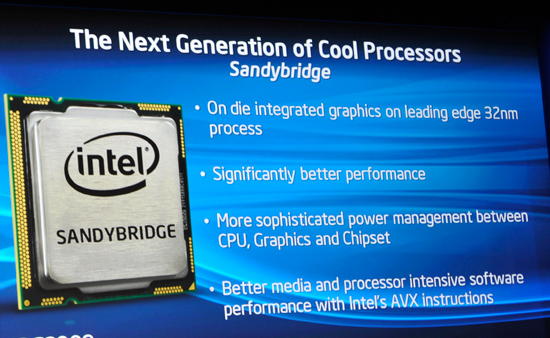
Both the CPU and GPU on SB will be able to turbo independently of one another. If you’re playing a game that uses more GPU than CPU, the CPU may run at stock speed (or lower) and the GPU can use the additional thermal headroom to clock up. The same applies in reverse if you’re running something computationally intensive.
On the CPU side little is known about the execution pipeline. Sandy Bridge enables support for AVX instructions, just like Bulldozer. The CPU will also have dedicated hardware video transcoding hardware to fend off advances by GPUs in the transcoding space.
Caches remain mostly unchanged. The L1 cache is still 64KB (32KB instruction + 32KB data) and the L2 is still a low latency 256KB. I measured both as still 4 and 10 cycles respectively. The L3 cache has changed however.
Only the Core i7 2600 has an 8MB L3 cache, the 2400, 2500 and 2600 have a 6MB L3 and the 2100 has a 3MB L3. The L3 size should matter more with Sandy Bridge due to the fact that it’s shared by the GPU in those cases where the integrated graphics is active. I am a bit puzzled why Intel strayed from the steadfast 2MB L3 per core Nehalem’s lead architect wanted to commit to. I guess I’ll find out more from him at IDF :)
The other change appears to either be L3 cache latency or prefetcher aggressiveness, or both. Although most third party tools don’t accurately measure L3 latency they can usually give you a rough idea of latency changes between similar architectures. In this case I turned to cachemem which reported Sandy Bridge’s L3 latency as 26 cycles, down from ~35 in Lynnfield (Lynnfield’s actual L3 latency is 42 clocks).
As I mentioned before, I’m not sure whether this is the result of a lower latency L3 cache or more aggressive prefetchers, or both. I had limited time with the system and was unfortunately unable to do much more.
And that’s about it. I can fit everything I know about Sandy Bridge onto a single page and even then it’s not telling us much. We’ll certainly find out more at IDF next month. What I will say is this: Sandy Bridge is not a minor update. As you’ll soon see, the performance improvements the CPU will offer across the board will make most anyone want to upgrade.


200 Comments
View All Comments
overzealot - Saturday, August 28, 2010 - link
Now, that's a name I've not heard in a long time. A long time.mapesdhs - Saturday, August 28, 2010 - link
Seems to be Intel is slowly locking up the overclocking scene because it has no
competition. If so, and Intel continues in that direction, then it would be a great
chance for AMD to win back overclocking fans with something that just isn't
locked out in the same way.
Looking at the performance numbers, I see nothing which suggests a product that
would beat my current 4GHz i7 860, except for the expensive top-end unlocked
option which I wouldn't consider anyway given the price.
Oh well, perhaps my next system will be a 6-core AMD.
Ian.
LuckyKnight - Saturday, August 28, 2010 - link
Do we have something more precise about the release date? Q1 is what - Jan/Feb/March/Apri?Looking to upgrade a core 2 duo at the moment - not sure whether to wait
mino - Saturday, August 28, 2010 - link
Q1 (in this case) means tricle amounts in Jan/Feb, mainstream availability Mar/April and worth-buying mature mobos in May/June timeframe.tatertot - Saturday, August 28, 2010 - link
Intel has already announced that shipments for revenue will occur in Q4 of this year. So, January launch.They've also commented that Sandy Bridge OEM demand is very strong, and they are adjusting the 32nm ramp up to increase supply. So January should be a decent launch.
Not surprising-- these parts have been in silicon since LAST summer.
chrsjav - Saturday, August 28, 2010 - link
Do modern clock generators use a quartz resonator? How would that be put on-die?iwodo - Saturday, August 28, 2010 - link
Since you didn't get this chip directly from Intel , i suspect there were no reviews guideline for you to follow, like which test to run and what test not to run etc.Therefore those benchmark from Games were not a results of special optimization in drivers. Which is great, because drivers matter much more then Hardware in GPU. If these are only early indication of what Intel new GPU can do, i expect there are more to extract from drivers.
You mention 2 Core GPU ( 12 EU ) verus 1 GPU ( 6 EU ), Any Guess as to what "E" stand for? And it seems like a SLI like tech rather then actually having more EU in one chip. The different being SLI or crossfire does not get any advantage unless drivers and games are working together. Which greatly reduces the chances of it working at full performance.
It also seems every one fail to realize one of the greatest performance will be coming from AVX. AVX will be like MMX again when we had the Pentium. I cant think of any other SSE having as great important to performance as AVX. Once software are specially optimize for AVX we should get another major lift in performance.
I also heard about rumors that 64bit in Sandy Bridge will work much better. But i dont know if there are anything we could test this.
The OpenCL sounds like a Intel management decision rather then a technical decision. May be Intel will provide or work with Apple to provide OpenCL on these GPU?
You also mention that Intel somehow support PCI -Express 2.0 with 1.0 performance. I dont get that bit there. Could you elaborate? 2.5GT/s for G45 Chipset??
If Intel ever decide to finally work on their drivers, then their GPU will be great for entry levels.
Are Dual Channel DDR3 1333 enough for Quad Core CPU + GPU? or even Dual core CPU.
Is GPU memory bandwidth limited?
Any update on Hardware Decoder? And what about transcoding part?
Would there be ways to lock the GPU to run at Turbo Clock all the time? Or GPU gets higher priority in Turbo etc..
How big is the Die?
P.S - ( Any news on Intel G3 SSD? i am getting worried that next Gen Sandforce is too good for intel. )
ssj4Gogeta - Saturday, August 28, 2010 - link
I believe EU means execution units.DanNeely - Sunday, August 29, 2010 - link
"You also mention that Intel somehow support PCI -Express 2.0 with 1.0 performance. I dont get that bit there. Could you elaborate? 2.5GT/s for G45 Chipset??"PCIE 2.0 included other low level protocol improvements in addition to the doubled clock speed. Intel only implemented the former; probably because the latter would have strangled the DMI bus.
"Are Dual Channel DDR3 1333 enough for Quad Core CPU + GPU? or even Dual core CPU."
Probably. The performance gains vs the previous generation isn't that large and it was enough for anything except pathological test cases (eg memory benchmarks). If it wasn't there'd be no reason why Intel couldn't officially support DDR3-1600 in their locked chipsets to give a bit of extra bandwidth.
chizow - Saturday, August 28, 2010 - link
@AnandCould you please clarify and expand on this comment please? Is this true for all Intel chipsets that claim support for PCIe 2.0?
[q]The other major (and welcome) change is the move to PCIe 2.0 lanes running at 5GT/s. Currently, Intel chipsets support PCIe 2.0 but they only run at 2.5GT/s, which limits them to a maximum of 250MB/s per direction per lane. This is a problem with high bandwidth USB 3.0 and 6Gbps SATA interfaces connected over PCIe x1 slots. With the move to 5GT/s, Intel is at feature parity with AMD’s chipsets and more importantly the bandwidth limits are a lot higher. A single PCIe x1 slot on a P67 motherboard can support up to 500MB/s of bandwidth in each direction (1GB/s bidirectional bandwidth).[/q]
If this is true, current Intel chipsets do not support PCIe 2.0 as 2.5GT/s and 250MB/s is actually the same effective bandwidth as PCIe 1.1. How did you come across this information? I was looking for ways to measure PCIe bandwidth but only found obscure proprietary tools not available publicly.
If Intel chipsets are only running at PCIe 1.1 regardless of what they're claiming externally, that would explain some of the complaints/concerns about bandwidth on older Intel chipsets.