Everything You Always Wanted to Know About SDRAM (Memory): But Were Afraid to Ask
by Rajinder Gill on August 15, 2010 10:59 PM ESTSynchronous dynamic random access memory (SDRAM) is made up of multiple arrays of single-bit storage sites arranged in a two-dimensional lattice structure formed by the intersection of individual rows (Word Lines) and columns (Bit Lines). These grid-like structures, called banks, provide an expandable memory space allowing the host control process and other system components with direct access to main system memory to temporarily write and read data to and from a centralized storage location.
When associated in groups of two (DDR), four (DDR2) or eight (DDR3), these banks form the next higher logical unit, known as a rank. 2GB DDR3 Dual Inline Memory Modules (DIMM) are undoubtedly the most popular density choice among today's enthusiast users. Most new parts of this type are configured as two identical ranks of eight banks each; one side of the DIMM housing those ICs that make up Rank 1, with Rank 2 populating the opposite face of the module. For this reason, single-sided DIMMs typically comprise only a single rank of addressable memory space.
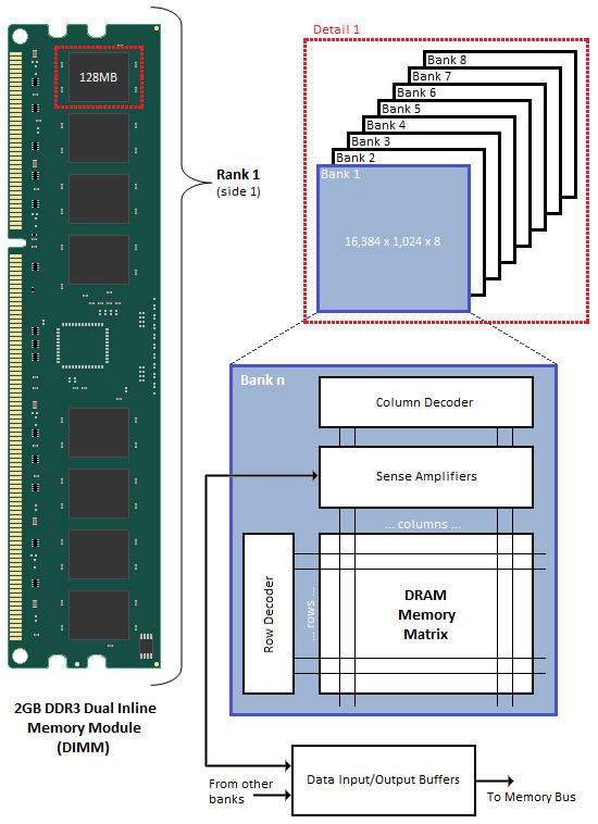
Figure 1 shows the typical functional arrangement of SDRAM memory space. In the case of our example dual-sided dual-rank unbuffered 2GB SDRAM DIMM, the fully populated module contains a total of 16 ICs, eight per side. Each IC contains eight banks of addressable memory space comprising 16K pages and 1K column address starting points with each column storing a single 8-bit word. This brings the total memory space to 128MB (16,384 rows/bank x 1,024 columns addresses/row x 1 byte/column address x 8 stacked banks) per IC. And since there are eight ICs per rank, Rank 1 is 1GB (128MB x 8 contiguous banks) in size, with the same for Rank 2, for a grand total of 2GB per module.
If each row contains 1K (1,024) column address staring points and each column stores 8 bits (1 byte), this would mean each row (page) is 8,192 bits (1,024 x 8 bits) or 1K bytes per bank. It's important to understand that each page of memory is segmented evenly across Bank n of each IC for the associated rank. For this reason, each page is in actuality 8KB (1KB x 8 contiguous banks) in size. So when we talk about IC density we are referring to eight distinct stacked banks and the total memory space therein, whereas when we talk about page space, we are really working with Bank n spread across the total number of ICs per rank. In the end the math comes out the same (8 ICs versus 8 banks), but conceptually it's a critical distinction worth acknowledging if we are to really grasp the ins and outs of memory addressing.
We can now see why the DDR3 core has a 8n-prefetch (where n refers to the number of banks per rank) as every read access to the memory requires a minimum of 64 bits (8 bytes) of data to be transferred. This is because each bank, of which there are eight for DDR3, fetches no less than 8 bits (1 byte) of data per read request - the equivalent of one column's worth of data. Whether or not the system actually makes use of all 8 bytes of transferred data is irrelevant. Any delivered data not actually requested can be safely disregarded as it's just a copy of what is still retained in memory.


46 Comments
View All Comments
ekoostik - Tuesday, August 17, 2010 - link
Great article. Going to take me a few more reads. One question - why no mention of Command Rate (and I double checked the Memory Scaling on Core i7 article, absent there too)? CR is often included in RAM specs, e.g. 9-9-9-24-2T, but never fully discussed if mentioned at all. Is it just not important anymore?Muhammed - Tuesday, August 17, 2010 - link
Ok I managed to royally confuse my self !What I know is that DDR3 operates at 1/8 the rated frequency , that means in case of DDR3 @800MHz , the internal memory operations are actually running at 100MHz , but the memory is able to fetch 8-words every clock cycle .
So 100MHz X (8 words ) = 800 Word per second as data rate , then the manufacturer misleadingly label the RAM module as a 800MHz part .
so the real benefit of DDR3 over DDR or DDR2 comes not from increased operating frequency , but from higher bandwidth .
To stress that fact , I mention DDR2 @800MHz , it operates at 200Mhz (internal clock) , however it only fetches 4-words every clock cycle , (200X4 = 800 Words).
When DDR3 operates at 200MHz (internal operations) like DDR2 , it fetches double the data , effectively managing 1600 words per second .
NOW , in your article .. you mention the base clock (I/o Bus) and you mention the double data rate , I know the I/O Bus clock is always 2 or 4 times the internal clock , so DDR3 @ 100MHz , has a 400MHz I/O bus .. but I couldn't understand the I/O bus function and it's relation in data transmission and data rate .
I am missing something here , could you enlighten me ?
Edison5do - Tuesday, August 17, 2010 - link
I Really was Affraid..!!Edison5do - Tuesday, August 17, 2010 - link
Technical Reading !!! LOve Thishasherr - Wednesday, August 18, 2010 - link
Great article. But what i dont get is how the hell motherboard knows all those timings? In SPDs there are like N timings described, isnt there really more? At least in bios settings i see more.Another thing. I buy Kingston 1800 MT/s module, with SPDs up to 1333 MTs. I overclock and make it run @ rated 1800mt/s speed. All timings are on auto. How the hell mobo/bios guess all of them :)?
ClagMaster - Wednesday, August 18, 2010 - link
Afraid to Ask ?After perusing through this I find myself afraid to read.
Comprehensive article for a novice EE
just4U - Wednesday, August 18, 2010 - link
Great article and ..." ....should be to focus development on reducing absolute minimum latency requirements for timings such as CAS and tRCD, rather than chasing.."
I hope the memory makers and shakers out there read that!!
lyeoh - Saturday, August 21, 2010 - link
The mistake counter bit counts seem OK to me. In what way are they wrong?There are 9 MSB (most significant bits) in the table.
Yes there are 13 bits in the counter, but the 9 bits in the table only refer to the 9 "top bits" of those 13 bits.
For example, if I have an 8 bit counter but 4 bits in some table only refer to the 4 most significant bits, then that means that you'd only see all zeroes in those 4 bits when the counter has values from 0 to 15 (0x0 to 0xF). When the counter has values from 240 to 255 (0xF0 to 0xFF), you'd see all ones in those 4 bits.
As for the description, I don't know the details of how the stuff works, so I don't know whether it's wrong or not.
dia - Saturday, August 21, 2010 - link
Read the explanation here:http://download.intel.com/design/processor/datasht...
Page 79.
To quote:
"MISTAKECOUNTER.
This field is the upper 8 MSBs of a 12-bit counter. This counter adapts the
interval between assertions of the page close flag. For a less aggressive page
close, the length of the count interval is increased and vice versa for a more
aggressive page close policy."
Now look at the left hand column, it shows 8:0. That's 9 bits! It's a 13 bit counter.
If it were a 12 bit counter the maximum permissible selection value would be 4095 and not 8191.
datasegment - Saturday, August 21, 2010 - link
Quick fyi - 8k is not 8196, it is 8192 :)