Arm Announces Mobile Armv9 CPU Microarchitectures: Cortex-X2, Cortex-A710 & Cortex-A510
by Andrei Frumusanu on May 25, 2021 9:00 AM EST- Posted in
- SoCs
- CPUs
- Arm
- Smartphones
- Mobile
- Cortex
- ARMv9
- Cortex-X2
- Cortex-A710
- Cortex-A510
The Cortex-A710: More Performance with More Efficiency
While the Cortex-X2 goes for all-out performance while paying the power and area penalties, Arm's Cortex-A710 design goes for a more efficient approach.
First of all, the new product nomenclature now is self-evident in regards to what Arm will be doing going forward- they’re skipping the A79 designation and simply starting fresh with a new three-digit scheme with the A710. Not very important in the grand scheme of things but an interesting marketing tidbit.
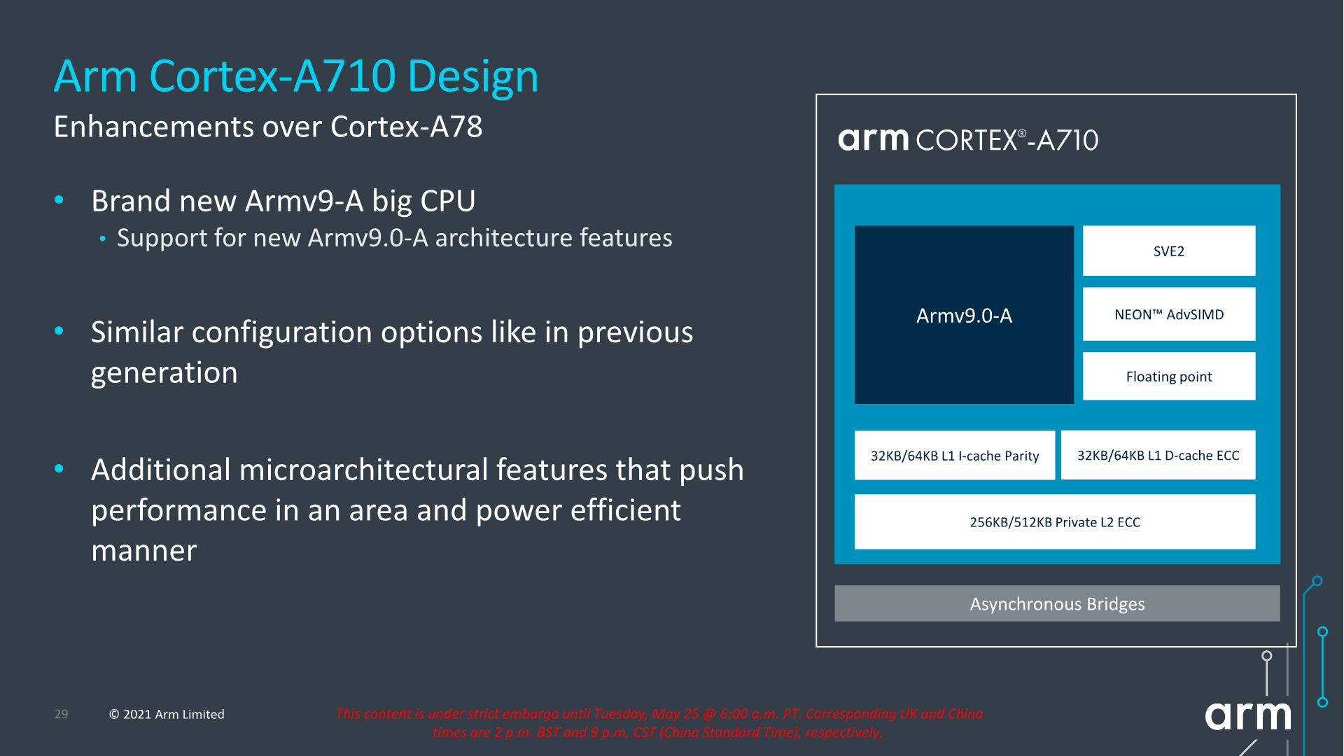
The Cortex-A710, much like the X2, is an Armv9 core with all new features that come with the new architecture version. Unlike the X2, the A710 also supports EL0 AArch32 execution, and as mentioned in the intro, this was mostly a design choice demanded by customers in the Chinese market where the ecosystem is still slightly lagging behind in moving all applications over to AArch64.
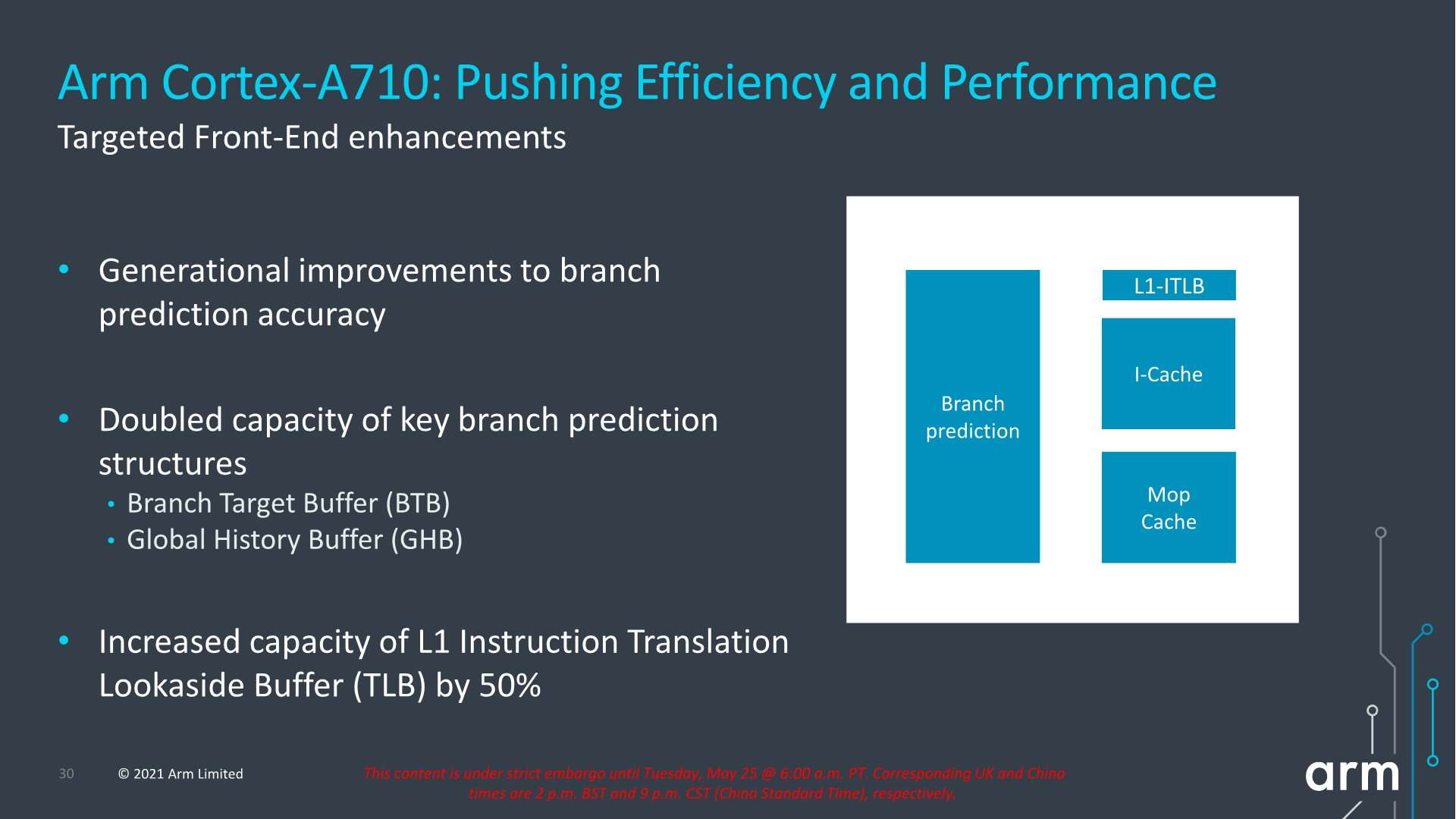
In terms of front-end enhancements, we’re seeing the same branch prediction improvements as on the X2, with larger structures as well as better accuracy. Other structures such as the L1I TLB have also seen an increase from 32 entries to 48 entries. Other front-end structures such as the macro-OP cache remain the same at 1.5K entries (The X2 also remains at 3K entries).
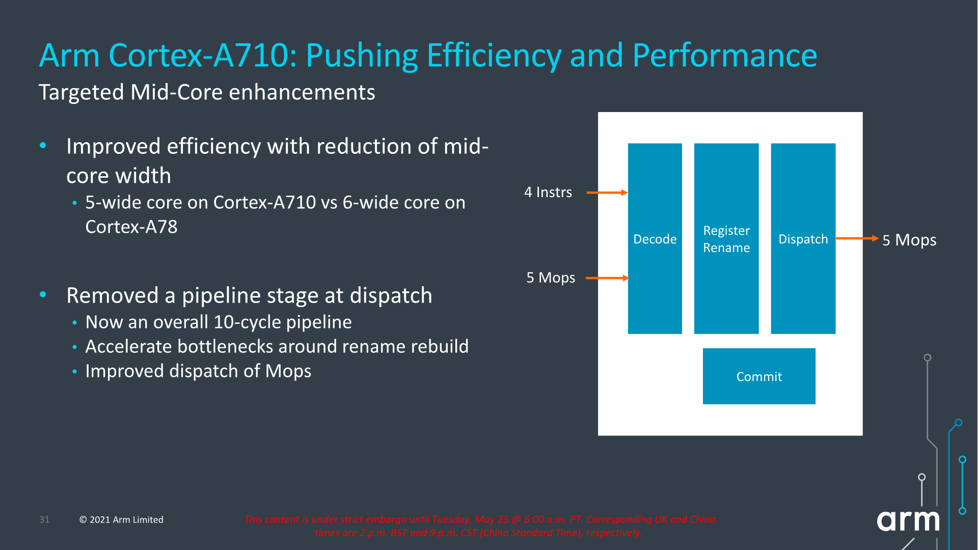
A very interesting choice for the A710 mid-core is that Arm has reduced the macro-OP cache and dispatch stage throughputs from 6-wide to 5-wide. This was mainly a targeted power and efficiency optimization for this generation, as we’re seeing a more important divergence between the Cortex-A and Cortex-X cores in terms of their specializations and targeted use-cases for performance and power.
The dispatch stage also features the same optimizations as on the X2, removing 1 cycle from the pipeline towards an overall 10-cycle pipeline design.
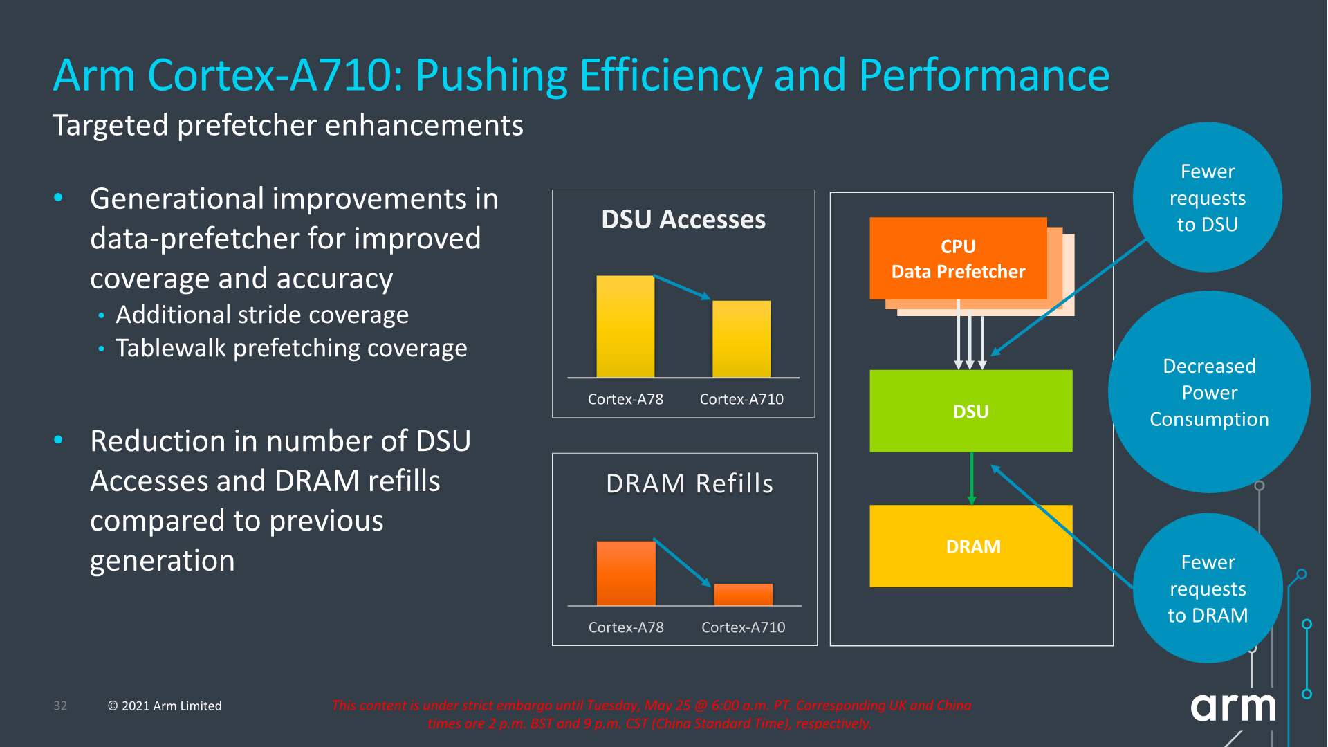
Arm also focuses on core improvements that affect the uncore parts of the system, which take place thanks to the new improvements in the prefetcher designs and how they interact with the new DSU-110 (which we’ll cover later). The new combination of core and DSU are able to reduce access from the core towards the L3 cache, as well as reducing the costly DRAM accesses thanks to the more efficiency prefetchers and larger L3 cache.
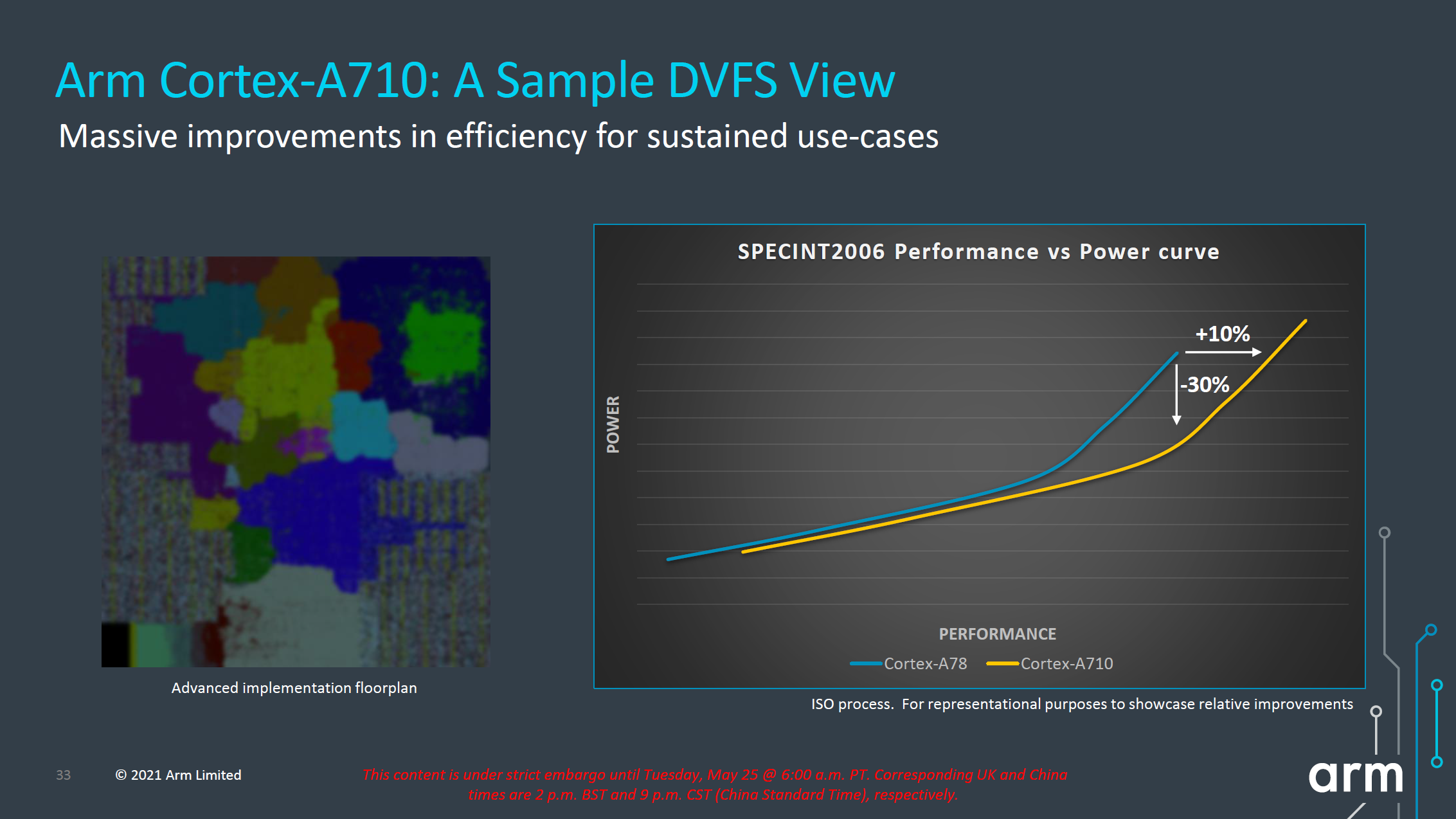
In terms of IPC, Arm advertises +10%, but again the issue with this figure here is that we’re comparing an 8MB L3 cache design to a 4MB L3 cache design. While this is a likely comparison for flagship SoCs next year, because the Cortex-A710 is also a core that would be used in mid-range or lower-end SoCs which might use much smaller L3 caches, it’s unlikely we’ll be seeing such IPC improvements in that sector unless the actual SoCs really do also improve their DSU sizes.
More important than the +10% improvement in performance is that, when backing off slightly in frequency, we can see that the power reduction can be rather large. According to Arm, at iso-performance the A710 consumes up to 30% less power than the Cortex-A78. This is something that would greatly help with sustained performance and power efficiency of more modestly clocked “middle” core implementations of the Cortex-A710.
In general, both the X2 and the A710’s performance and power figures are quite modest, making them the smallest generation-over-generation figures we’ve seen from Arm in quite a few years. Arm explains that due to this generation having made larger architectural changes with the move to Armv9, there has been an impact in regards to the usual efficiency and performance improvements that we’ve seen in prior generations.
Both the X2 and the A710 are also the fourth generation of this Austin microarchitecture family, so we’re hitting a wall of diminishing returns and maturity of the design. A few years ago we were under impression that the Austin family would only go on for three generations before handing things over to a new clean-sheet design from the Sophia team, but that original roadmap has been changed, and now we'll be seeing the new Sophia core with larger leaps in performance being disclosed next year.


181 Comments
View All Comments
ChrisGX - Thursday, May 27, 2021 - link
Using Andrei's initial performance estimate for the X1 (clocked at 3GHz) as a guide (47.2 SPECint2006) and ARM's own projection for the peak performance boost offered by the X2 over the X1 (+30% when process optimisations and frequency increases are factored in) we get a rating of 61.4 SPECint2006 for next years X series core. That is really a best case estimate and it is where the good news ends.The information we have on the 2022 Cortex cores does seem to lack the transparency of material of this sort that had been issued in earlier years by ARM. It is disappointing not to have any core frequency data in that information. A lot turns on realistic estimations of attainable core frequencies and having a good sense of power dissipation at maximum burst frequencies. We now know that Andrei's performance estimate for the X1 core wasn't borne out in practice (the actual performance exhibited by the highest performing X1 core - the one in the Snapdragon 888 - was 14% lower at 41.3 SPECint2006) owing to pitiful power dissipation characteristics of Samsung's 5nm LPE process that in order to prevent thermal build up and keep power consumption within budget on SoCs incorporating an X1 core SoC designers found it necessary to either a) reduce burst clock frequencies to below 3GHz or b) use restrictive power management controls to damp down chip operations threatening the thermal stability of the SoC that will naturally have the effect of throttling performance.
Using more realistic assumptions to project the likely performance of the X2 core (which I suspect might still be too optimistic because these forthcoming SoCs that incorporate an X2 core like the flagship Android smartphone SoCs of 2021 are said to be scheduled for production on Samsung fabs which must cast a degree of doubt on ARM's performance projections because recently Samsung's silicon process technologies have demonstrably failed to come up tp ARM's expectations) we get this number: 53.7 SPECint2006 (which represents the actual performance of the highest performing X1 core of 2021 x 1.3). Given the lack of transparency in the ARM data it is possible to entertain a rather broad range of imaginable SPEC peak integer performance ratings for the X2 core. A SPECspeed of 53.7 is my best guess.
ikjadoon - Tuesday, May 25, 2021 - link
These are geometric means of integer & FP scores. Typo for X1, ~50 not ~40. Let's be precise, now that I'm not on a phone ;)SPEC2006 1T Geomean:
A14 Firestorm = 71.72 points
A13 Lightning = 59.09 points
SD888 X1 = 49.48 points
Awarding the X2 the full 16% jump on both integer & FP, we can napkin math this to a Reference X2 = 57.40 at iso-frequency.
You're right they can (and maybe should) boost clocks so it could surpass the A13, but it's unrealistic to imagine Qualcomm shipping a 3.3+ GHz smartphone in 2022, especially if it's Samsung foundries again, but even on TSMC. Qualcomm's SD888 X1 at 2.84 GHz already ate 9621 joules (SPECint2006) and 4972 joules (SPECfp2006).
From https://www.anandtech.com/show/16463/snapdragon-88...
No one expects a literal doubling, but Arm's competition (NUVIA, Apple, Ampere) are not slowing down, either.
Wilco1 - Tuesday, May 25, 2021 - link
OK I get it now - the 40 made me think you meant SPECINT as that is what Cortex-X1 scored.3.3GHz on TSMC 5nm is conservative given it has significant performance/power improvements (which the A14 already benefits from), but yes it means switching back to TSMC.
Thala - Tuesday, May 25, 2021 - link
Indeed the performance gains of A14 vs. A13 are mostly frequency driven and much less IPC driven. It is not unreasonable to assume some frequency gains for X2 as well when moving to 5nm TSMC.Ppietra - Wednesday, May 26, 2021 - link
Thala, looking at the numbers IPC improved 8%, being responsible for 42% of performance growth... so not exactly much less!A13 to A14 transition gives no clue about what would happen between X1 and X2 or between Samsung and TSMC... X1 is already at 5nm, and its clock speed is just 5% less than the A14... Their designs priorities are also different, so you cannot infer much!
name99 - Tuesday, May 25, 2021 - link
All true. But of course A14 is an especially easy opponent!- it's the last round of what appears to be Apple's 4-year "seriously new micro-architecture" cadence -- A77..A10 as gen 1, A11..A14 as gen 2, A15 et seq as gen 3.
- it was clearly designed with the single highest priority being get the x86 stuff working. Meaning that anything that did not match that priority (including, eg, optimized physical layout and risky micro-architectural innovations) was punted till the A15
- it doesn't have SVE/2, which is good for anything up to a 80% speed boost depending on the exact code (even with just compiler vectorization). Averaging over "representative code bases" is a game that's never going to get everyone to agree, but the one attempt I saw to do this came up with an average performance boost of ~30%.
Given how *low* ARM's numbers are, I assume they're talking about performance in the absence of use of SVE/2? Honestly the whole thing is kinda weird, how little they're pushing the SVE/2 angle and how much one might expect it to improve things.
I do *not* expect Apple to be as timid... And while Apple tend to shy away from hardware announcements at WWDC, we all know about M1 by now, AND we know that SVE/2 will be in next year's ARM (so presumably in this year's Apple). Meaning maybe there will be some talks about SVE/2 (and other ARMv9 stuff) at WWDC?
Wilco1 - Tuesday, May 25, 2021 - link
You are exaggerating the gains of SIMD in general. Yes automatic vectorization helps, but even if it improves some image transformations by 80%, it's never going to speed up browsing by 30%. Or any other general purpose code. Or SPEC.Remember this is 128-bit SVE, so 4 Neon units are about as fast as 4 SVE units. For great SVE performance on HPC code look at A64FX or the upcoming Neoverse V1.
name99 - Tuesday, May 25, 2021 - link
- One hopes that the combination of agnostic length and predicates will allow a lot of code for which vectorization was previously uneconomical (too expensive to mask out fiddly bits, too much overhead in loop prologs and epilogs) to now be handled. We shall see.- You are right about the 128b of course; yet another instance of ARM never trying for a stretch goal! I assume Apple will be implementing this as 2x256, meaning, among other things, the path from L1D to LSU grows from 128b to 256b wide, and that's an example of where SVE/2 (indirectly, sure) helps boost performance for everyone.
smalM - Friday, May 28, 2021 - link
Could you please explain why you asume Apple will reduce the number of FP/SIMD units in exchange for widening them. Is that really better? From a FP or from a SIMD standpoint?Thanks in advance.
Making the path from L1D to LSU 256b wide is something Apple could do anyways and is not directly related to SVE2; I was astonished they didn't do it when they added the fourth FP/NEON unit.
mode_13h - Saturday, May 29, 2021 - link
> would you please explain why you asume Apple will reduce the number of FP/SIMD units> in exchange for widening them. Is that really better?
For SVE it's a little better, since it means software having to run loops for about half as many iterations, correspondingly reducing loop overhead.
> Making the path from L1D to LSU 256b wide is something Apple could
> do anyways and is not directly related to SVE2
I don't really see why. It seems like it'd only help for back-to-back reads or writes from/to consecutive addresses. And if 128-bits is already enough to do that, then extra width would be a waste.