Arm Announces Mobile Armv9 CPU Microarchitectures: Cortex-X2, Cortex-A710 & Cortex-A510
by Andrei Frumusanu on May 25, 2021 9:00 AM EST- Posted in
- SoCs
- CPUs
- Arm
- Smartphones
- Mobile
- Cortex
- ARMv9
- Cortex-X2
- Cortex-A710
- Cortex-A510
The Cortex-X2: More Performance, Deeper OoO
We first start off with the Cortex-X2, successor to last year’s Cortex-X1. The X1 marked the first in a new IP line-up from Arm which diverged its “big” core offering into two different IP lines, with the Cortex-A sibling continuing Arm’s original design philosophy of PPA, while the X-cores are allowed to grow in size and power in order to achieve much higher performance points.
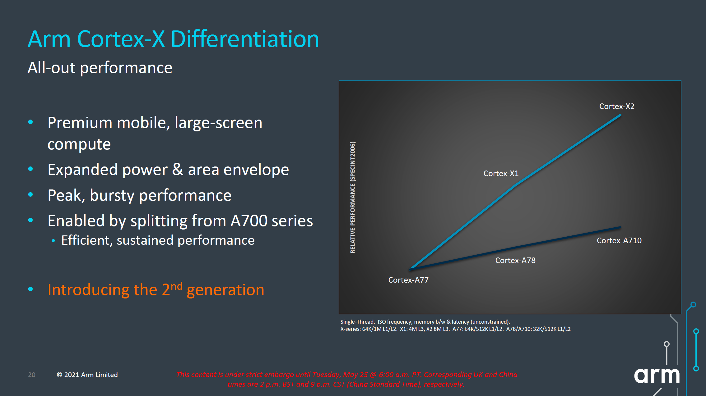
The Cortex-X2 continues this philosophy, and further grows the performance and power gap between it and its “middle” sibling, the Cortex-A710. I also noticed that throughout Arm’s presentation there were a lot more mentions of having the Cortex-X2 being used in larger-screen compute devices and form-factors such as laptops, so it might very well be an indication of the company that some of its customers will be using the X2 more predominantly in such designs for this generation.
From an architectural standpoint the X2 is naturally different from the X1, thanks in large part to its support for Armv9 and all of the security and related ISA platform advancements that come with the new re-baselining of the architecture.
As noted in the introduction, the Cortex-X2 is also a 64-bit only core which only supports AArch64 execution, even in PL0 user mode applications. From a microarchitectural standpoint this is interesting as it means Arm will have been able to kick out some cruft in the design. However as the design is a continuation of the Austin family of processors, I do wonder if we’ll see more benefits of this deprecation in future “clean-sheet” big cores designs, where AArch64-only was designed from the get-go. This, in fact, is something that's already happening in other members of Arm's CPU cores, as the new little core Cortex-A510 was designed sans-AArch32.
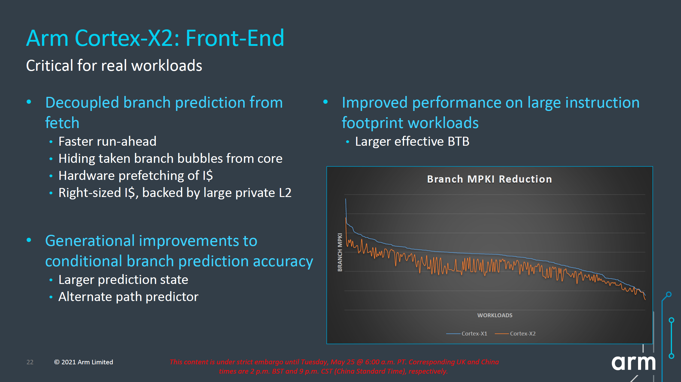
Starting off with the front-end, in general, Arm has continued to try to improve what it considers the most important aspect of the microarchitecture: branch prediction. This includes continuing to run the branch resolution in a decoupled way from the fetch stages in order to being able to have these functional blocks be able to run ahead of the rest of the core in case of mispredicts and minimize branch bubbles. Arm generally doesn’t like to talk too much details about what exactly they’ve changed here in terms of their predictors, but promises a notable improvement in terms of branch prediction accuracy for the new X2 and A710 cores, effectively reducing the MPKI (Misses per kilo instructions) metric for a very wide range of workloads.
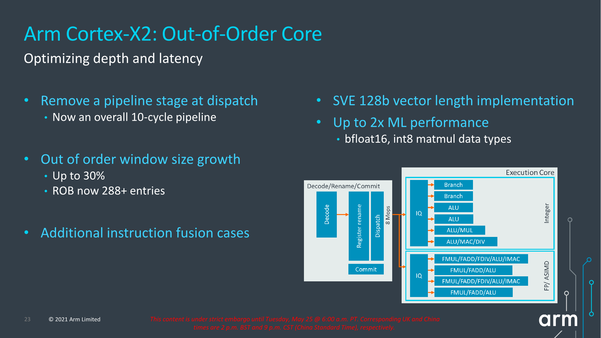
The new core overall reduces its pipeline length from 11 cycles to 10 cycles as Arm has been able to reduce the dispatch stages from 2-cycles to 1-cycle. It’s to be noted that we have to differentiate the pipeline cycles from the mispredict penalties, the latter had already been reduced to 10 cycles in most circumstances in the Cortex-A77 design. Removing a pipeline stage is generally a rather large change, particularly given Arm’s target of maintaining frequency capabilities of the core. This design change did incur some more complex engineering and had area and power costs; but despite that, as Arm explains in, cutting a pipeline stage still offered a larger return-on-investment when it came to the performance benefits, and was thus very much worth it.
The core also increases its out-of-order capabilities, increasing the ROB (reorder buffer) by 30% from 224 entries to 288 entries this generation. The effective figure is actually a little bit higher still, as in cases of compression and instruction bundling there are essentially more than 288 entries being stored. Arm says there’s also more instruction fusion cases being facilitated this generation.
On the back-end of the core, the big new change is on the part of the FP/ASIMD pipelines which are now SVE2-capable. In the mobile space, the SVE vector length will continue to be 128b and essentially the new X2 core features similar throughput characteristics to the X1’s 4x FP/NEON pipelines. The choice of 128b vectors instead of something higher is due to the requirement to have homogenous architectural feature-sets amongst big.LITTLE designs as you cannot mix different vector length microarchitectures in the same SoC in a seamless fashion.
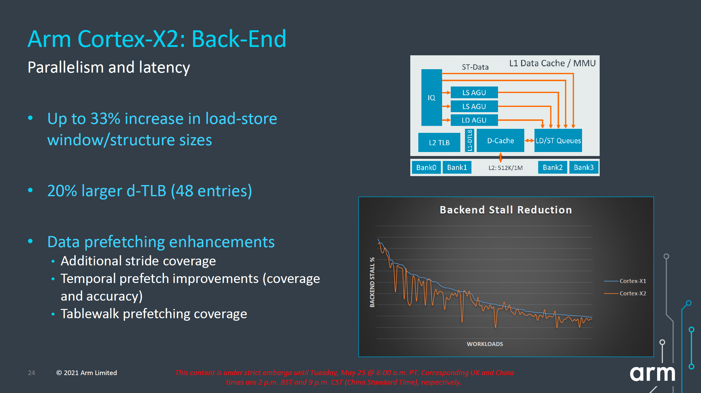
On the back-end, the Cortex-X2 continues to focus on increasing MLP (memory level parallelism) by increasing the load-store windows and structure sizes by 33%. Arm here employs several structures and generally doesn’t go into detail about exactly which queues have been extended, but once we get our hands on X2 systems we’ll be likely be able to measure this. The L1 dTLB has grown from 40 entries to 48 entries, and as with every generation, Arm has also improved their prefetchers, increasing accuracies and coverage.
One prefetcher that surprised us in the Cortex-X1 and A78 earlier this year when we first tested new generation devices was a temporal prefetcher – the first of its kind that we’re aware of in the industry. This is able to latch onto arbitrary repeated memory patterns and recognize new iterations in memory accesses, being able to smartly prefetch the whole pattern up to a certain depth (we estimate a 32-64MB window). Arm states that this coverage is now further increased, as well as the accuracy – though again the details we’ll only able to see once we get our hands on silicon.
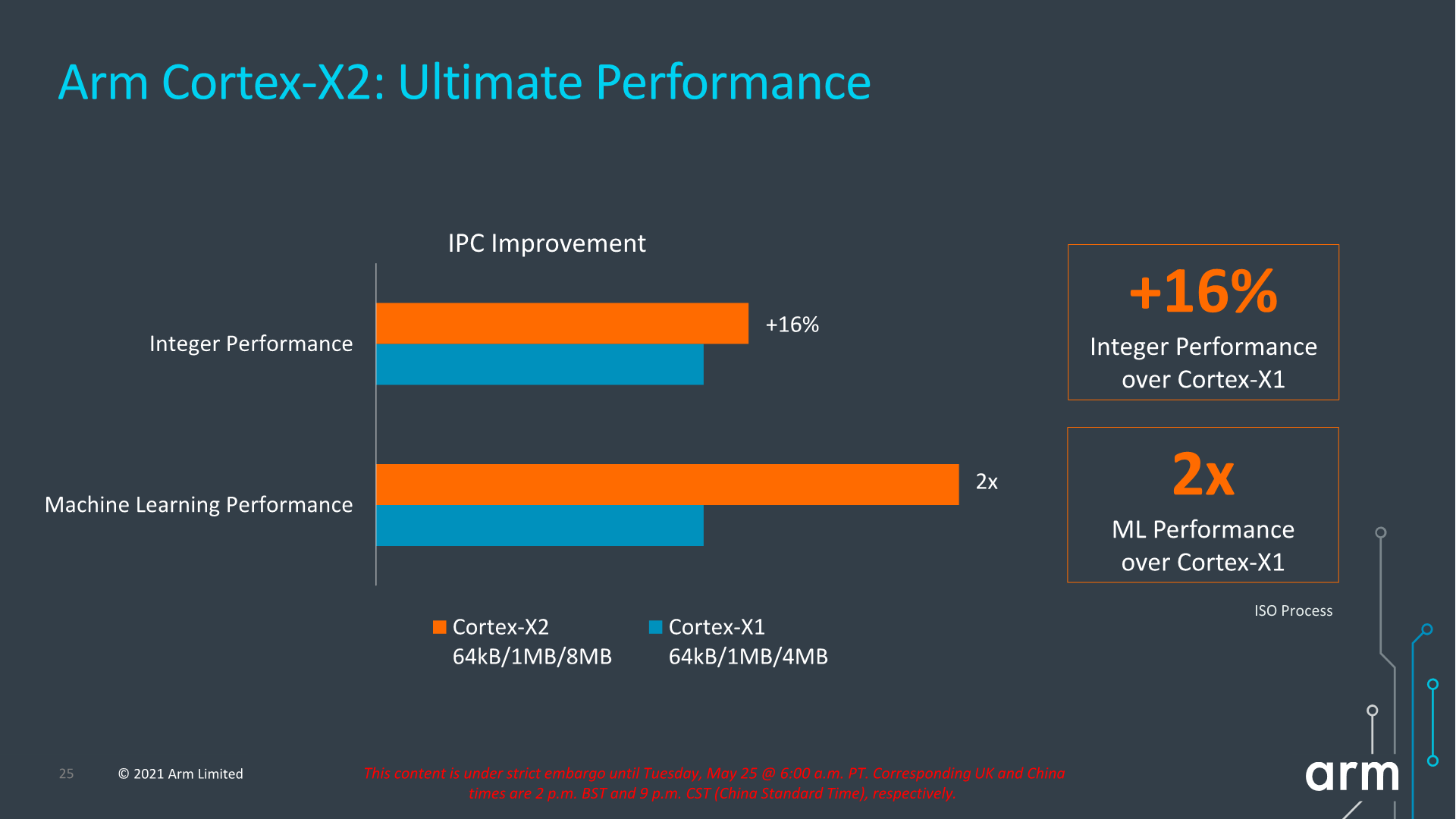
In terms of IPC improvements, this year’s figures are quoted to reach +16% in SPECint2006 at ISO frequency. The issue with this metric (and which applies to all of Arm’s figures today) is that Arm is comparing an 8MB L3 cache design to a 4MB L3 design, so I expect a larger chunk of that +16% figure to be due to the larger cache rather than the core IPC improvements themselves.
For their part, Arm is reiterating that they're expecting 8MB L3 designs for next year’s X2 SoCs – and thus this +16% figure is realistic and is what users should see in actual implementations. But with that said, we had the same discussion last year in regards to Arm expecting 8MB L3 caches for X1 SoCs, which didn't happen for either the Exynos 2100 nor the Snapdragon 888. So we'll just have to wait and see what cache sizes the flagship commercial SoCs end up going with.

In terms of the performance and power curve, the new X2 core extends itself ahead of the X1 curve in both metrics. The +16% performance figure in terms of the peak performance points, though it does come at a cost of higher power consumption.
Generally, this is a bit worrying in context of what we’re seeing in the market right now when it comes to process node choices from vendors. We’ve seen that Samsung’s 5LPE node used by Qualcomm and S.LSI in the Snapdragon 888 and Exynos 2100 has under-delivered in terms of performance and power efficiency, and I generally consider both big cores' power consumption to be at a higher bound limit when it comes to thermals. I expect Qualcomm to stick with Samsung foundry in the next generation, so I am admittedly pessimistic in regards to power improvements in whichever node the next flagship SoCs come in (be it 5LPP or 4LPP). It could well be plausible that we wouldn’t see the full +16% improvement in actual SoCs next year.


181 Comments
View All Comments
ChrisGX - Thursday, May 27, 2021 - link
Using Andrei's initial performance estimate for the X1 (clocked at 3GHz) as a guide (47.2 SPECint2006) and ARM's own projection for the peak performance boost offered by the X2 over the X1 (+30% when process optimisations and frequency increases are factored in) we get a rating of 61.4 SPECint2006 for next years X series core. That is really a best case estimate and it is where the good news ends.The information we have on the 2022 Cortex cores does seem to lack the transparency of material of this sort that had been issued in earlier years by ARM. It is disappointing not to have any core frequency data in that information. A lot turns on realistic estimations of attainable core frequencies and having a good sense of power dissipation at maximum burst frequencies. We now know that Andrei's performance estimate for the X1 core wasn't borne out in practice (the actual performance exhibited by the highest performing X1 core - the one in the Snapdragon 888 - was 14% lower at 41.3 SPECint2006) owing to pitiful power dissipation characteristics of Samsung's 5nm LPE process that in order to prevent thermal build up and keep power consumption within budget on SoCs incorporating an X1 core SoC designers found it necessary to either a) reduce burst clock frequencies to below 3GHz or b) use restrictive power management controls to damp down chip operations threatening the thermal stability of the SoC that will naturally have the effect of throttling performance.
Using more realistic assumptions to project the likely performance of the X2 core (which I suspect might still be too optimistic because these forthcoming SoCs that incorporate an X2 core like the flagship Android smartphone SoCs of 2021 are said to be scheduled for production on Samsung fabs which must cast a degree of doubt on ARM's performance projections because recently Samsung's silicon process technologies have demonstrably failed to come up tp ARM's expectations) we get this number: 53.7 SPECint2006 (which represents the actual performance of the highest performing X1 core of 2021 x 1.3). Given the lack of transparency in the ARM data it is possible to entertain a rather broad range of imaginable SPEC peak integer performance ratings for the X2 core. A SPECspeed of 53.7 is my best guess.
ikjadoon - Tuesday, May 25, 2021 - link
These are geometric means of integer & FP scores. Typo for X1, ~50 not ~40. Let's be precise, now that I'm not on a phone ;)SPEC2006 1T Geomean:
A14 Firestorm = 71.72 points
A13 Lightning = 59.09 points
SD888 X1 = 49.48 points
Awarding the X2 the full 16% jump on both integer & FP, we can napkin math this to a Reference X2 = 57.40 at iso-frequency.
You're right they can (and maybe should) boost clocks so it could surpass the A13, but it's unrealistic to imagine Qualcomm shipping a 3.3+ GHz smartphone in 2022, especially if it's Samsung foundries again, but even on TSMC. Qualcomm's SD888 X1 at 2.84 GHz already ate 9621 joules (SPECint2006) and 4972 joules (SPECfp2006).
From https://www.anandtech.com/show/16463/snapdragon-88...
No one expects a literal doubling, but Arm's competition (NUVIA, Apple, Ampere) are not slowing down, either.
Wilco1 - Tuesday, May 25, 2021 - link
OK I get it now - the 40 made me think you meant SPECINT as that is what Cortex-X1 scored.3.3GHz on TSMC 5nm is conservative given it has significant performance/power improvements (which the A14 already benefits from), but yes it means switching back to TSMC.
Thala - Tuesday, May 25, 2021 - link
Indeed the performance gains of A14 vs. A13 are mostly frequency driven and much less IPC driven. It is not unreasonable to assume some frequency gains for X2 as well when moving to 5nm TSMC.Ppietra - Wednesday, May 26, 2021 - link
Thala, looking at the numbers IPC improved 8%, being responsible for 42% of performance growth... so not exactly much less!A13 to A14 transition gives no clue about what would happen between X1 and X2 or between Samsung and TSMC... X1 is already at 5nm, and its clock speed is just 5% less than the A14... Their designs priorities are also different, so you cannot infer much!
name99 - Tuesday, May 25, 2021 - link
All true. But of course A14 is an especially easy opponent!- it's the last round of what appears to be Apple's 4-year "seriously new micro-architecture" cadence -- A77..A10 as gen 1, A11..A14 as gen 2, A15 et seq as gen 3.
- it was clearly designed with the single highest priority being get the x86 stuff working. Meaning that anything that did not match that priority (including, eg, optimized physical layout and risky micro-architectural innovations) was punted till the A15
- it doesn't have SVE/2, which is good for anything up to a 80% speed boost depending on the exact code (even with just compiler vectorization). Averaging over "representative code bases" is a game that's never going to get everyone to agree, but the one attempt I saw to do this came up with an average performance boost of ~30%.
Given how *low* ARM's numbers are, I assume they're talking about performance in the absence of use of SVE/2? Honestly the whole thing is kinda weird, how little they're pushing the SVE/2 angle and how much one might expect it to improve things.
I do *not* expect Apple to be as timid... And while Apple tend to shy away from hardware announcements at WWDC, we all know about M1 by now, AND we know that SVE/2 will be in next year's ARM (so presumably in this year's Apple). Meaning maybe there will be some talks about SVE/2 (and other ARMv9 stuff) at WWDC?
Wilco1 - Tuesday, May 25, 2021 - link
You are exaggerating the gains of SIMD in general. Yes automatic vectorization helps, but even if it improves some image transformations by 80%, it's never going to speed up browsing by 30%. Or any other general purpose code. Or SPEC.Remember this is 128-bit SVE, so 4 Neon units are about as fast as 4 SVE units. For great SVE performance on HPC code look at A64FX or the upcoming Neoverse V1.
name99 - Tuesday, May 25, 2021 - link
- One hopes that the combination of agnostic length and predicates will allow a lot of code for which vectorization was previously uneconomical (too expensive to mask out fiddly bits, too much overhead in loop prologs and epilogs) to now be handled. We shall see.- You are right about the 128b of course; yet another instance of ARM never trying for a stretch goal! I assume Apple will be implementing this as 2x256, meaning, among other things, the path from L1D to LSU grows from 128b to 256b wide, and that's an example of where SVE/2 (indirectly, sure) helps boost performance for everyone.
smalM - Friday, May 28, 2021 - link
Could you please explain why you asume Apple will reduce the number of FP/SIMD units in exchange for widening them. Is that really better? From a FP or from a SIMD standpoint?Thanks in advance.
Making the path from L1D to LSU 256b wide is something Apple could do anyways and is not directly related to SVE2; I was astonished they didn't do it when they added the fourth FP/NEON unit.
mode_13h - Saturday, May 29, 2021 - link
> would you please explain why you asume Apple will reduce the number of FP/SIMD units> in exchange for widening them. Is that really better?
For SVE it's a little better, since it means software having to run loops for about half as many iterations, correspondingly reducing loop overhead.
> Making the path from L1D to LSU 256b wide is something Apple could
> do anyways and is not directly related to SVE2
I don't really see why. It seems like it'd only help for back-to-back reads or writes from/to consecutive addresses. And if 128-bits is already enough to do that, then extra width would be a waste.