Arm Announces Mobile Armv9 CPU Microarchitectures: Cortex-X2, Cortex-A710 & Cortex-A510
by Andrei Frumusanu on May 25, 2021 9:00 AM EST- Posted in
- SoCs
- CPUs
- Arm
- Smartphones
- Mobile
- Cortex
- ARMv9
- Cortex-X2
- Cortex-A710
- Cortex-A510
The Cortex-A710: More Performance with More Efficiency
While the Cortex-X2 goes for all-out performance while paying the power and area penalties, Arm's Cortex-A710 design goes for a more efficient approach.
First of all, the new product nomenclature now is self-evident in regards to what Arm will be doing going forward- they’re skipping the A79 designation and simply starting fresh with a new three-digit scheme with the A710. Not very important in the grand scheme of things but an interesting marketing tidbit.
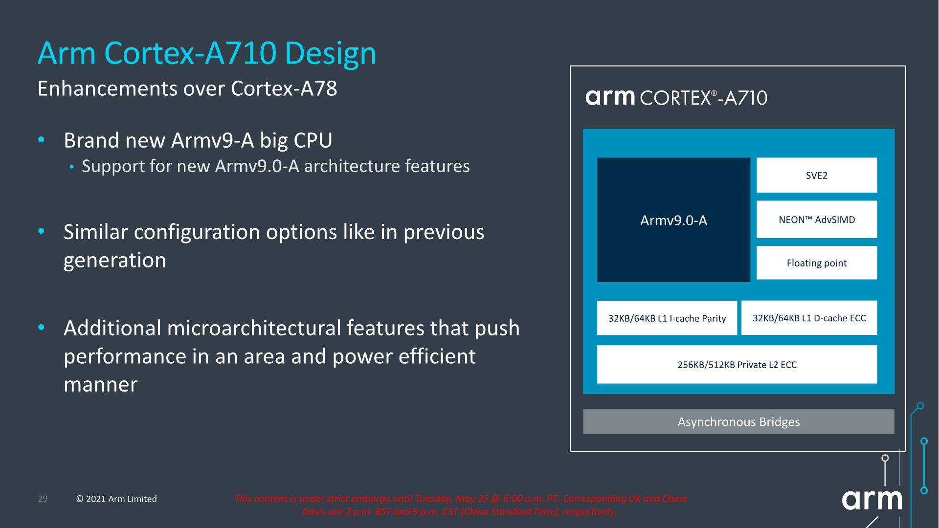
The Cortex-A710, much like the X2, is an Armv9 core with all new features that come with the new architecture version. Unlike the X2, the A710 also supports EL0 AArch32 execution, and as mentioned in the intro, this was mostly a design choice demanded by customers in the Chinese market where the ecosystem is still slightly lagging behind in moving all applications over to AArch64.
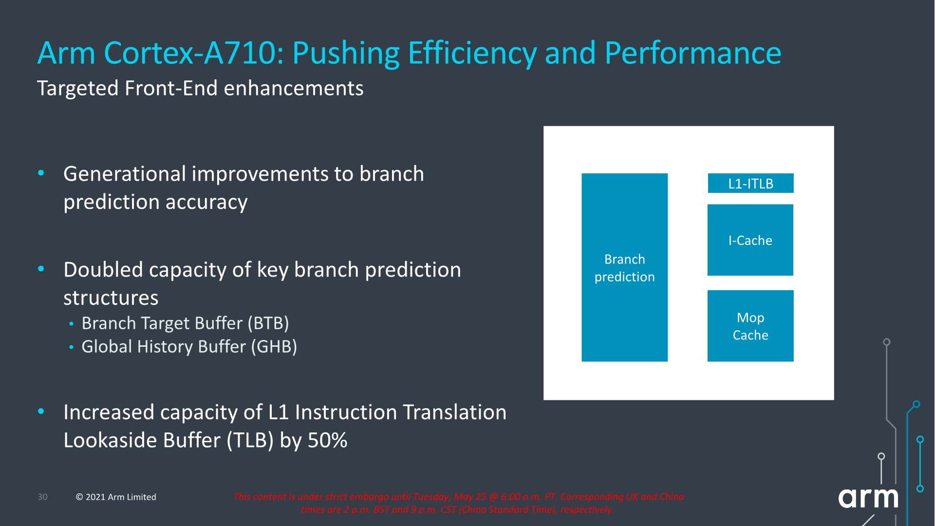
In terms of front-end enhancements, we’re seeing the same branch prediction improvements as on the X2, with larger structures as well as better accuracy. Other structures such as the L1I TLB have also seen an increase from 32 entries to 48 entries. Other front-end structures such as the macro-OP cache remain the same at 1.5K entries (The X2 also remains at 3K entries).
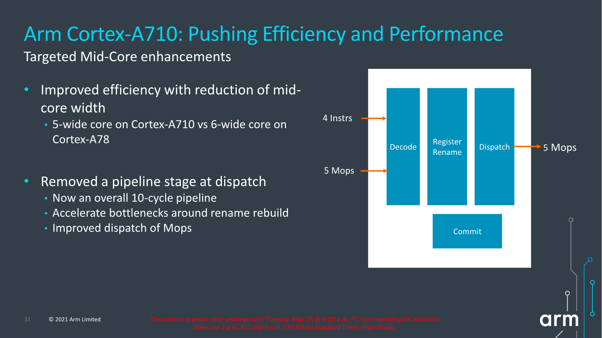
A very interesting choice for the A710 mid-core is that Arm has reduced the macro-OP cache and dispatch stage throughputs from 6-wide to 5-wide. This was mainly a targeted power and efficiency optimization for this generation, as we’re seeing a more important divergence between the Cortex-A and Cortex-X cores in terms of their specializations and targeted use-cases for performance and power.
The dispatch stage also features the same optimizations as on the X2, removing 1 cycle from the pipeline towards an overall 10-cycle pipeline design.
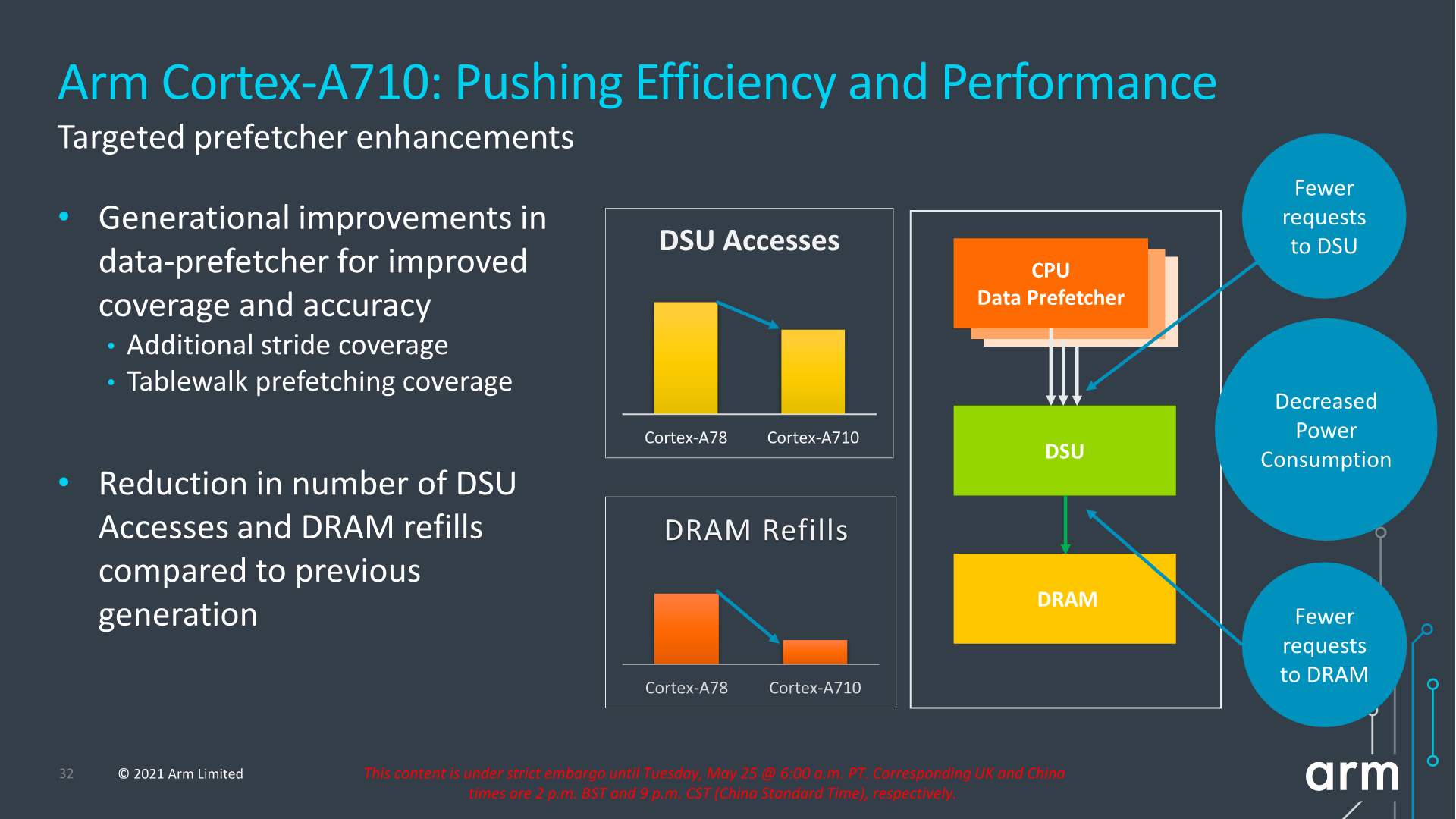
Arm also focuses on core improvements that affect the uncore parts of the system, which take place thanks to the new improvements in the prefetcher designs and how they interact with the new DSU-110 (which we’ll cover later). The new combination of core and DSU are able to reduce access from the core towards the L3 cache, as well as reducing the costly DRAM accesses thanks to the more efficiency prefetchers and larger L3 cache.
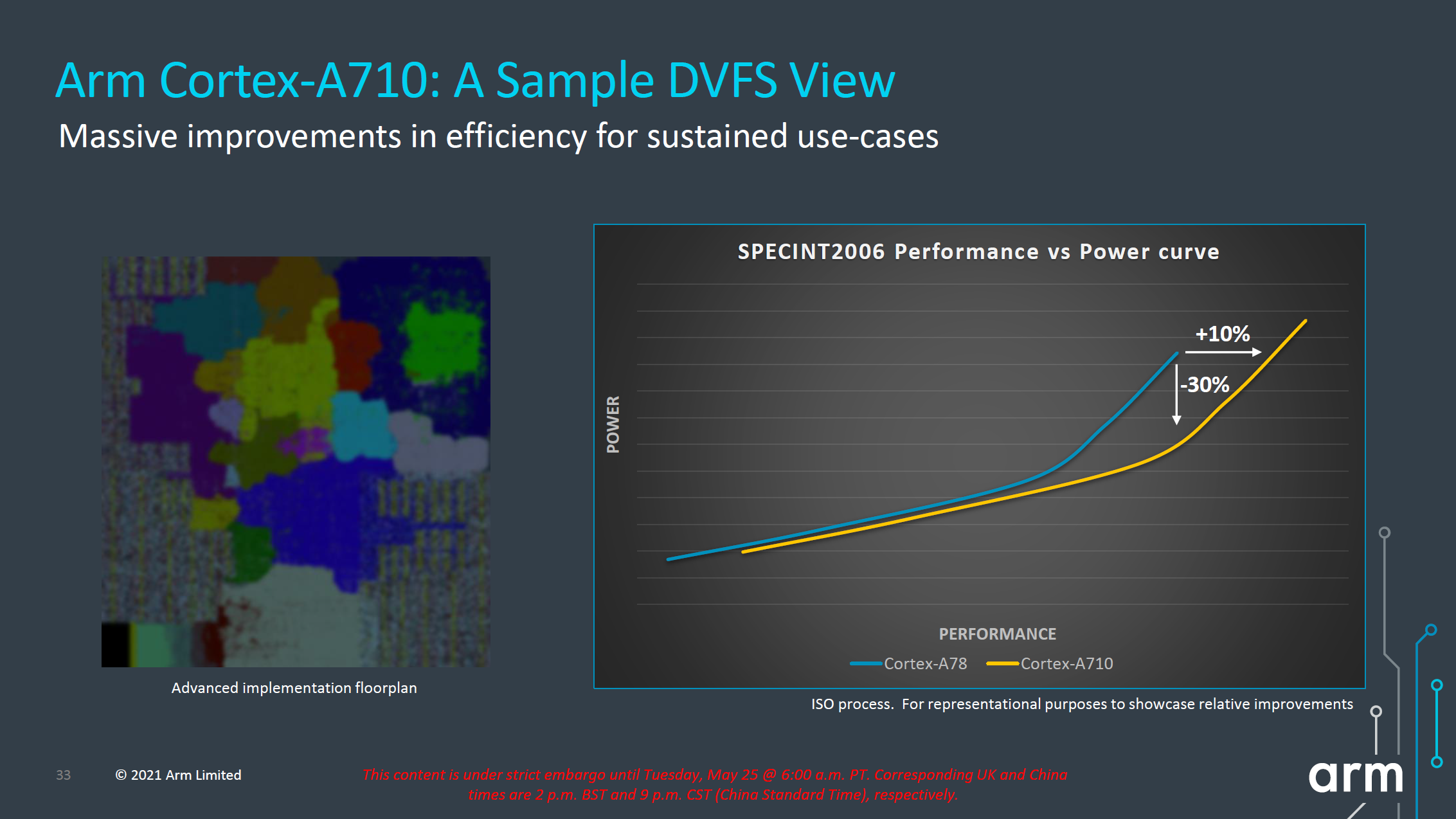
In terms of IPC, Arm advertises +10%, but again the issue with this figure here is that we’re comparing an 8MB L3 cache design to a 4MB L3 cache design. While this is a likely comparison for flagship SoCs next year, because the Cortex-A710 is also a core that would be used in mid-range or lower-end SoCs which might use much smaller L3 caches, it’s unlikely we’ll be seeing such IPC improvements in that sector unless the actual SoCs really do also improve their DSU sizes.
More important than the +10% improvement in performance is that, when backing off slightly in frequency, we can see that the power reduction can be rather large. According to Arm, at iso-performance the A710 consumes up to 30% less power than the Cortex-A78. This is something that would greatly help with sustained performance and power efficiency of more modestly clocked “middle” core implementations of the Cortex-A710.
In general, both the X2 and the A710’s performance and power figures are quite modest, making them the smallest generation-over-generation figures we’ve seen from Arm in quite a few years. Arm explains that due to this generation having made larger architectural changes with the move to Armv9, there has been an impact in regards to the usual efficiency and performance improvements that we’ve seen in prior generations.
Both the X2 and the A710 are also the fourth generation of this Austin microarchitecture family, so we’re hitting a wall of diminishing returns and maturity of the design. A few years ago we were under impression that the Austin family would only go on for three generations before handing things over to a new clean-sheet design from the Sophia team, but that original roadmap has been changed, and now we'll be seeing the new Sophia core with larger leaps in performance being disclosed next year.


181 Comments
View All Comments
Ppietra - Tuesday, May 25, 2021 - link
I believe that he was talking about the overall SPEC2006 score and not just SPECint. Still he would be wrong about the X1 score, which would be 50 and not 40 (probably a typo).Anyway a 16% improvement for X2 over X1 would mean a score of 58 which, like he said, would still be behind the A13 performance core and well behind the 72 score for the A14.
X1 is already being manufactured at 5nm, so it makes no sense to factor in a transition from 7nm.
Wilco1 - Tuesday, May 25, 2021 - link
Cortex-X1 can reach 3.2GHz in Samsung's 5nm process but the power is too high: https://images.anandtech.com/doci/16463/2100-volta...TSMC 5nm is faster and lower power, which allows for higher frequencies. At a conservative 3.3GHz X2 would have a combined score of ~66.7 (only 7% slower than A14).
Ppietra - Tuesday, May 25, 2021 - link
That is not how it works!First of all you have no idea what would be the advantage from using TSMC instead of Samsung, so you are just throwing numbers with no substance. Secondly, X1 energy consumption is already very high (it is less efficient than the A14 Firestorm core), so no, there doesn’t seem to be a lot of room to improve X2 clock speed to 3.3GHz. Thirdly even with your assumption you would still have X2 performing worse than a 1 year old core
Wilco1 - Tuesday, May 25, 2021 - link
We absolutely do know. TSMC 5nm is ~15% faster than 7nm at the same power (or 30% lower power at the same frequency). We know that SD865+ achieves 3.1GHz on 7nm and that the frequency gain from A13 on 7nm to A14 on 5nm was around 13%. So 3.3GHz should be feasible on 5nm without increasing power.The point is that TSMC 5nm will give a significant perf/power boost (that A14 already benefits from). And that means the gap has narrowed to only one generation rather than 2.
melgross - Tuesday, May 25, 2021 - link
It’s not that simple. The cores would require a bit of a redesign for the different process, and each design would fare differently. Some might get a good boost, and others may not.michael2k - Tuesday, May 25, 2021 - link
You're comparing the X2 to the A14? I mean, if we're lucky we will see the X2 in 2022 alongside the A16. The A15 will be released this year, in 2021. We already have some X1 baselines:https://www.anandtech.com/show/16463/snapdragon-88...
So in terms of generation:
2021 X1 not competitive with the 2019 A13 now
2021 X1 competitive with the 2019 A13 on TSMC 5nm
2021 X1 not competitive with the 2021 A15 (est 10% boost to hit 70 SPECint)
2022 X2 competitive with the 2020 A14 on TSMC 5nm
2022 X2 not competitive with the 2021 A15
That still sounds like a 2 generation gap to me. The real problem isn't fundamentally the core, but the OEM choosing not to use a 2x2 design (2 X1 and 2 A77) or (2 X2 and 2 A710), so even if the cores get faster each generation, overall performance is hobbled by using 3 medium cores instead of a pair of higher performance X1 or X2 cores.
Fulljack - Wednesday, May 26, 2021 - link
it's cat and mouse, really. Apple release their phones in late Q3, while Samsung S-series are released in late Q1. there's 5 to 6 month difference.Ppietra - Wednesday, May 26, 2021 - link
Nothing of what you said gives you any data to infer about a transition from Samsung to TSMC.SD865+ does not use a X1 core, as such you have no commonality to make that kind jump in analysis, secondly the X1 core already consumes significantly more than the SD865+ core, so clearly there is no much room to increase clock speed from that perspective. If you want to increase clock speed you need to keep power consumption under control.
Wilco1 - Wednesday, May 26, 2021 - link
These are different generations of the same microarchitecture from the same design team with the same frequency capability (as reported by AnandTech). So yes there is obvious commonality.We also know this microarchitecture is capable of higher frequencies, for example AnandTech reports Cortex-X1 can reach 3.2GHz. The main problem is power however, which is what limited Cortex-X1 on Samsung's process. TSMC 5nm reduces power by 30% which enables higher clock speeds.
Ppietra - Wednesday, May 26, 2021 - link
actually they aren’t different generations from the same microarchitecture. The next generation for the A77 is the A78. The X1 goes for a bigger core design, and as such consumes more.Being capable of higher frequencies doesn't mean that Qualcomm (, etc) finds it viable to use those higher frequencies in a smartphone SoC...
NODE power reduction is stated for same performance and microarchitecture (which X1 is not) and only as an internal TSMC comparison... The data you give tells you nothing about X1 (already at 5nm) transitioning to TSMC. You are making an analysis based on wrong assumptions.