Samsung Announces 3nm GAA MBCFET PDK, Version 0.1
by Dr. Ian Cutress on May 14, 2019 8:00 PM EST- Posted in
- Semiconductors
- Samsung
- 3nm
- GAAFET
- MBCFET
_678x452.jpg)
So what comes after 7nm, after 6nm, after 5nm, and after 4nm? That's right: 3nm! At Samsung's Foundry Forum event today, Samsung has announced that the first alpha version of its Product Design Kit for its first 3nm process is now ready for customers. What makes this announcement special is that 3nm is the intersection point where Samsung intends to introduce the next generation of Gate-All-Around (GAA) technology that will replace FinFETs.
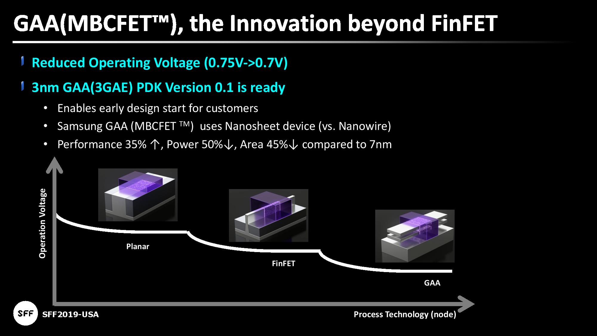
Beyond the FinFET: Moving to Gate-All-Around
The main driver for innovation in logic-based process technologies over the past decade has been FinFETs. Compared to a standard planar transistor, the FinFET allowed for better performance and voltage scaling as the process node decreased, minimizing the negative aspects of transistor limitations. FinFETs work by increasing the contact area between the channel of the transistor and the gate by scaling in a vertical direction, allowing for faster switching times and higher current density compared to a planar design.
However, like planar transistors, FinFET transistors eventually reach a point where they cannot scale as process nodes shrink. In order to scale, that contact area between the channel and the gate needs to increase, and the way to do this is to use a Gate-All-Around (GAA) design. GAA adjusts the dimensions of the transistor to ensure that the gate is also below the channel, not only on the top and the sides. This allows a GAA design to stack transistors vertically, rather than laterally.
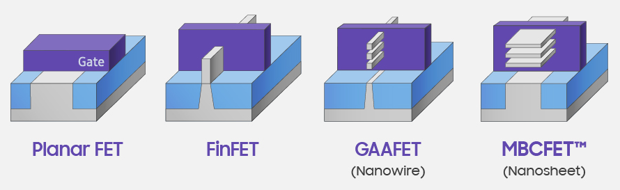
GAA based FETs (GAAFETs) can come in a variety of form factors. Most of the research has pointed to nanowire based GAAFETs, with a small channel width and making the channel as small as possible. These type of GAAFETs are typically useful for low power designs, but are hard to manufacture. The other implementation is making the channel like a horizontal sheet, increasing the volume of the channel, which affords benefits towards performance and scaling. This nano-sheet based GAAFET is what Samsung is calling a Multi-Bridge Channel FET, or MBCFET, which is going to be a trademarked name for the company.
Where planar transistors scaled to around 22nm/16nm, FinFETs have been ideal as we go down from 22nm/14nm to 5nm and 4nm. Samsung is planning to introduce nano-sheet based GAAFETs on its 3nm design, replacing FinFETs entirely.
Building on 3nm: PDKs
When a semiconductor company designs a new chip on a given process, one of the tools they need is a design kit from the foundry then plan to use. For anyone creating an Arm chip on 14nm chip today for example, they would call up Arm and ask for the Cortex-A55 design kit for Samsung or TSMC or GlobalFoundries, which has been optimized for that process. For 14nm, these design kits are very mature, and Arm is likely to offer different versions depending if you want a high frequency or a low power optimization.
However when a process technology is new, early alpha and beta versions of these product design kits (PDKs) become available. The PDK contains the design rules for the process, as well as optimizations that are used to make the best for power and performance. Typically the foundry will update the PDK as more chips are produced and more variations are tested to help its customers make the best chips.
The Nuance with MBCFETs
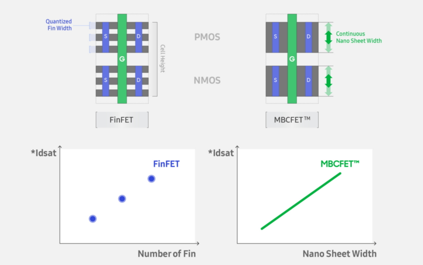
One of the features of MCBFETs that wasn’t specifically listed in Samsung’s press release is that nano-sheet based FETs are extremely customizable. The width of the nanosheet is a key metric in defining the power and performance characteristics: the higher the width, the higher the performance (at higher power). Samsung has included in its PDK four different nanosheet widths in order to provide co-optimization within the same chip design: transistor designs that focus on low power can use smaller nanosheets, while logic that requires higher performance can go for the wider sheets, but ultimately it's a continuous scale. By contrast, FinFETs only have one power/frequency design point within a process node design for a given fin count, creating only discrete profiles possible.
Samsung states that its 3GAE design, regardless of the sheet width design required, will allow for direct IP porting from any of its 4nm family designs. 3GAE and 4LPP share the same BEOL design rules, enabling this.
Samsung Announces 3nm GAA MBCFET PDK, Version 0.1
Today’s announcement is that Samsung is offering its first alpha version of the PDK for its first generation 3nm process that uses MBCFETs. Samsung is calling this process its ‘3GAE’ process, and this alpha version will allow its partners to start getting to grips with some of the new design rules for its 3GAE process.
Samsung is making a lot of promises with its first 3GAE process. One of the headlines is lowering the operating voltage from 0.75 volts to 0.70 volts, which will be a good step in power. The headline PPA values that Samsung is announcing are also impressive: compared to 7nm, 3GAE will offer 1.35x performance, 0.5x power, with a 0.65x die area.
Samsung states that these performance numbers are based on using larger width cells for critical paths where frequency is important, and smaller width cells for non-critical paths where power savings are crucial. Technically Fmax of the widest cells is listed as 1.5x, while power at Fmax is 0.6x. Power at iso-performance is where the 0.5x number comes from.
To put some of this in perspective: Samsung expects its 3GAE process to offer first customer tapeouts in 2020, with risk production in late 2020 and volume manufacturing in late 2021.
Beyond 3GAE, Samsung has already outlined that its second generation 3nm process will be called 3GAP, with a focus on high performance operation. The 3GAP process will be optimization focused, taking advantage of what Samsung has learned from 3GAE. 3GAE will go into risk production in 2021, with mass production likely in 2022.
PDK Tools and EDA Partners
For those that are interested, the PDK tools includes SPICE, DRC, LVS, PEX, P-Cell, Fill Deck, and P&R Techfile. EDA Partners include Cadence, Mentor, and Synopsys.
Related Reading
- Samsung to Invest $115 Billion in Foundry & Chip Businesses by 2030
- Samsung Completes Development of 5nm EUV Process Technology
- Samsung Foundry Roadmap: EUV-Based 7LPP for 2018, 3 nm Incoming
- Samsung Foundry Updates: 8LPU Added, EUVL on Track for HVM in 2019
- Samsung Starts Mass Production of Chips Using Its 7nm EUV Process Tech


32 Comments
View All Comments
name99 - Wednesday, May 15, 2019 - link
Samsung claim that they started fabbing something (undisclosed) in high volume 7nm towards the end of 2018. There are a few reasonable possibilities, like Tesla (their chip is Samsung, nothing more disclosed) or maybe one of the various NN companies that have sprung up.5nm and 4nm are somewhat like 7nm+ and 7nm++, so reasonable products for say late 2019/early 2020 and mid 2021. Then 3nm late 2022. It's not an unreasonable schedule.
Samsung is not (as far as I know) discussing a 6nm. That's TSMC, for whom 6nm is more or less their 7nm++ for next year (7nm+ is this year's process). It will run in parallel with TSMC 5nm, but of course these are foundries --- part of their business model is to run simultaneously multiple processes at different performance/cost tradeoffs.
SaberKOG91 - Wednesday, May 15, 2019 - link
Don't forget that as EUV matures it will be involved in more of the process steps which is hopefully where a lot of these gains will come from. EUV was still extremely expensive when 7nm first launched to it was used in very few "bullet-proof" steps.Rudde - Wednesday, May 15, 2019 - link
Tesla NN-accelerator is 14nm.attila123 - Sunday, January 19, 2020 - link
You are taiwanese arn't you? You guys are funny. Samsung and Hynex was bust with their supercycle with their dram and nand chips. EVU Samsung went right into. TSMC Still using FINFIT. Just using EUV here and here. Don't get too Cocky dude. Samsung jsut went made a revolutionary feat which was in very much doubt. Stop being a troll because you are jealous. Just give them what they deserve. They accomplish something. That's it. You tone sucks and you're angy Samsung got there before Taiwan. EUV right away didn't work wout. But after the supercycle, they will cocentrate on the SOC which they already have. I didn't hear TSMC doing anything with EUV before Samsung brought it in. So just stop being a trollSychonut - Wednesday, May 15, 2019 - link
Looking forward to Intel's 14+++++.boeush - Wednesday, May 15, 2019 - link
Looking forward to Samsung's first subatomic-scale node.watersb - Wednesday, May 15, 2019 - link
Great write-up.I am really confused by these node names: how do they compare with Intel? What, exactly, is the "3 nanometer" aspect of the process?
Santoval - Wednesday, May 15, 2019 - link
They cannot be compared via nm numbers because these are purely marketing numbers. One more objective way of comparison is via transistor density, i.e. the number of transistors per mm^2. Even that can be fudged though, because for instance SRAM caches have different transistor density than the logic part of a chip.An ideal way of third party comparison of the density of different nodes would be to compare the density of the exact same chip (CPU or GPU) fabbed at say 14nm and 7nm. If you know the total number of transistors of the chips (which should be identical) you can then measure the bare dies to calculate their size (in square mm) and then divide the total transistor number by the die sizes to get the transistor density per mm^2.
HStewart - Wednesday, May 15, 2019 - link
In some ways you can think of Samsung 3nm here as Samsung 7nn++++. But the real determination is the number of transistors per size and speed between each device. Not sire if other foundries will have something similar to Intel Foreros which is not to confused with EMiB, where the die is 3d direction which increases the components in the vertical direction.I believe a storm is coming with this technology, it does not mean that this 3nm will be replace, but it could mean one of component in the Foreros package could be 3nm based - say if Samsung comes out with dense ram chips.I believe that Foveros is a revolution not evolution in technology. But it is designed to complement the process technology not replace it.
ajc9988 - Sunday, May 26, 2019 - link
Foveros is NOT a revolution. It is just 3D stacking. The most impressive part of it is the moving of a cache layer to the active interposer-ish base that the chiplets are attached to for it. Other than that, it is just the evolution of 2.5D, which AMD has had whitepapers detailing the analysis on cost of implementation back around November or December of 2017.So, to have something competitive, all they would need to do is incorporate components of their I/O die onto the active interposer and place HBM centrally stacked with the core chiplets around. Now, Intel being able to stack eDRAM for a level 4 cache sitting above the hotter components is a step forward, but other companies have looked into that as well and the entire industry has been moving toward that. They don't have a major lead on anyone in that regards. Also, they are only using it at first in extremely low power devices, which is where heat from core chiplets is easier to manage. Implementation in high performance chips will take more time because of that.
So, a 2.5D will likely be used in a high performance setting before 3D integrations. Whether Intel, AMD, or some other player will do so is just a matter of seeing who wins that race. But this isn't as revolutionary as you make it seem. It is an incremental step.