Xilinx Announces Project Everest: The 7nm FPGA SoC Hybrid
by Ian Cutress on March 19, 2018 7:40 AM EST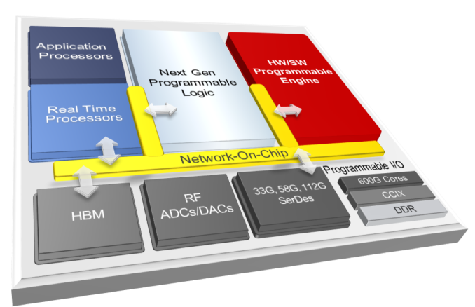
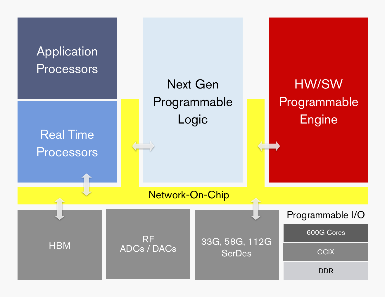
This week Xilinx is making public its latest internal project for the next era of specialized computing. The new product line, called Project Everest in the interim, is based around what Xilinx is calling an ACAP – an Adaptive Compute Acceleration Platform. The idea here is that for both compute and acceleration, particularly in the data center, the hardware has to be as agile as the software. Project Everest will combine Xilinx’s highest performing next-generation programmable logic along with application processors, real-time processors, programmable engines, RF, high-speed SerDes, programmable IO, HBM, and a custom network-on-chip. The idea is that space typically devoted to hard blocks in FPGAs (such as memory controllers) are now optimized on chip, leaving more programmable silicon for the compute and adaptability. Project Everest is one of the Three Big Trends as identified by Xilinx’s new CEO, Victor Peng.
Turn to Page 2 to see our interview of Xilinx CEO, Victor Peng
An Adaptive Compute Acceleration Platform: Project Everest
For most of the consumer market, CPUs and GPUs take up most of the processing within a system. In the data center, FPGAs are also used as a third level of compute, typically as an agile processor to assist with acceleration, and the premise is that it can be configured on the fly for an optimized compute pathway without having to spend tens of millions to create custom chips or ASICs. If an FPGA were to emulate a CPU or a GPU, it would ultimately be slower or draw more power, but typically the way CPUs and GPUs are configured are not always the best pathways for a lot of compute, and FPGAs are typically used as network accelerators or as a hub for things like semi-conductor design, emulating how other chips are built, or novel cryptographic compute workloads. If you need an FPGA with more memory for example, then the programmable logic can construct a memory controller, such that an embedded implementation with a PHY will give access to more memory. Of course, this is a simplification.
FPGAs, are by design, PCIe co-processors, much like GPUs. The workflow is somewhat similar as well after the circuit is designed: develop the code and run the data through using APIs. In recent product cycles, Xilinx has bundled new features to its FPGA line, such as hardened memory controllers supporting HBM, and embedded Arm Cortex cores for application-specific programmability. What Project Everest aims to bring to the table is another form of processing unit, combining a number of features but going beyond the current CPU/GPU/FPGA paradigm: the Adaptive Compute Acceleration Platform (or ACAP).
Xilinx’s ACAP portfolio will be initiated with TSMC’s 7nm manufacturing process, with the first tapeouts due in late 2018. Xilinx states that Project Everest has been a monumental internal effort, taking 4-5 years and 1500 engineers already, with over $1b in R&D costs. The final big chips are expected to weigh in at 50 billion transistors, with a mix of monolithic and interposer designs based on configurations.
Today’s announcement is more of a teaser than anything else – the diagram above is about the limit to which that Xilinx will talk about features and the product portfolio. The value of the ACAP, according to Xilinx, will be its feature set and millisecond-level configurability. For a server on the edge, for example, an ACAP can use both the programmable logic elements for millisecond bitstream reconfiguration of different processes along with the application processors for general logic or the programmable engines as ASIC-level acceleration. This can lead to, among other things, different AI acceleration techniques and 5G RF manageability by multiple containers/VMs on a single ACAP. The overriding idea is that the ACAP can apply dynamic optimization for workloads, with Xilinx citing a 10-100x speedup over CPUs and more use cases than GPUs or ASICs as a fundamental value to the new hardware, built through software and hardware programmability. Xilinx also stated that the RF will have four times the bandwidth of current 16nm radios, leveraging 16x16 800 MHz radios.
Xilinx did mention two specific features that will be coming to Project Everest. The chips will have ASIC-level blocks for CCIX connectivity – a cache coherent interconnect that promises to be the ‘one bus to rule them all’ (quote from Charlie at SemiAccurate), although Xilinx does not go into direct detail about the bandwidth. Xilinx does however mention its SerDes capability, going up to 112G PAM-4, which Xilinx demonstrated only this week at an Optical Fiber Conference. Xilinx did not state whether Project Everest will use integrated or external transceivers, however, and we will have to wait for a bigger announcement later in the year.
The ultimate goal, according to Xilinx, is for the ACAP to be a universal accelerator. The six areas that Xilinx provided as examples were for live streaming, sensor analytics, AI speech services, social video screening, financial modelling, and personalized medicine: the idea is that the ACAP can tackle all of these on the fly as a result of its feature set, hardware and software programmability, embedded connectivity, and onboard accelerators.
Xilinx is still formulating a brand name for its Project Everest products, and as mentioned above, there is expected to be a range of monolithic and interposer enabled options. Tapeout is expected in 2018, with products in 2019, using TSMC’s 7nm. This means that the first products are likely to be the high-performance, high-margin numbers. Xilinx has no direct plans at this time to bring the ACAP strategy back to 16nm or larger. Key strategic customers are already engaging Xilinx on the project.
Xilinx Tackling the Software Problem
If my employer told me to go take a week, do a course and learn a new skill, it would be to learn how to use FPGAs. I was never exposed to them much during my academic career, especially when GPUs were only just coming through as the compute platform of choice for parallelizable code. Since FPGAs and FPGA-like devices hit the market, one thing has been clear – the user has to be more of a hardware engineer than a software engineer to get to grips with them. Xilinx has seen this as a sizable barrier for entry for its product line, and part of the revised methodology under new CEO Victor Peng is to enable a new wave of users by reducing this barrier.
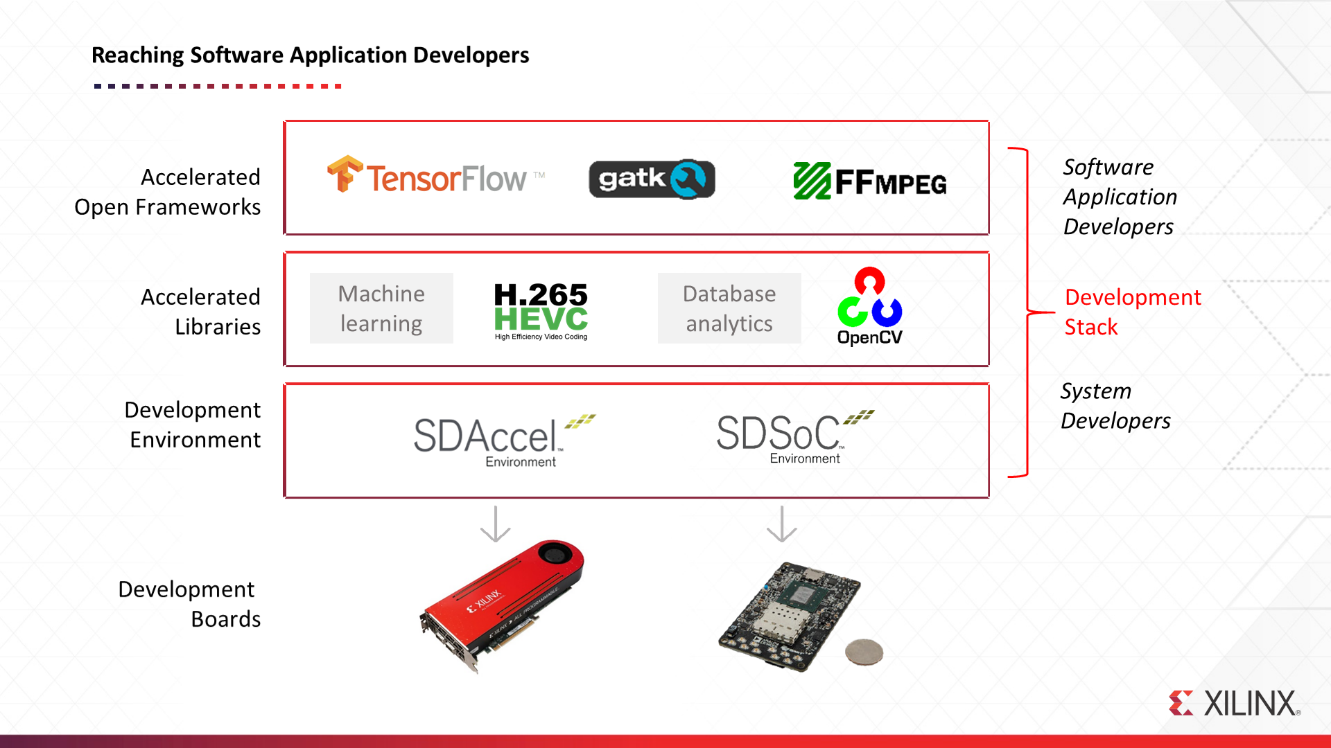
One of the topics in our briefing discussed alongside Everest was how to drive that new generation. The goal, according to Xilinx, is to get developers used to the FPGA as ‘just another PCIe co-processor, like a GPU’, and enable it to be programmed as such. As a result, Xilinx is pursuing a strategy of accelerated libraries, much like what has happened in the GPU space. The ultimate goal is that a developer can take a library, which has the necessary resources to configure a bit-stream on the fly and implement it to the hardware at hand, and just use it – all the FPGA reconfiguration happens at a level below what the software developer needs. So far Xilinx has been working on accelerating AI frameworks, codecs, machine learning, and database analytics, in this way. Developers still have to target the SDAccel and SDSoC software development environments, but it was clear that enabling this higher level of users is in Xilinx’s portfolio for the future, especially when an ACAP can be hardware and software configurable.
Xilinx 2018: The Focus
The briefing we had on Project Everest, because it still is early for the product line, was ultimately a chance for the company to introduce the new CEO. Bundled with this were a reformation of Xilinx’s priorities within the presentation and discussions. We have an interview with Victor Peng on the next page, but it is worth at least enumerating how Xilinx is set to approach its future.
Xilinx’s key headline that it is focusing on being a ‘Data Center First’ company. We were told that the company is now focused on the data center as its largest growth potential, as compared to its regular customer base, the time to revenue is rapid, the time to upgrade (for an FPGA company) is rapid, and it enables a fast evolution of customer requirements and product portfolio. Peng stated that Xilinx is a company that can approach compute, storage, and networking, and have a product for all three. Part of the key to being a major data center player will be the software, as discussed in the section above, but also connections with technology such as CCIX, and enablement through service providers with ‘FPGA as a Service (FaaS)’ in cloud infrastructures. Xilinx cites enterprise customers already deployed and using their hardware to afford a 40x inference speedup, a 90x analytics speedup, and a 100x genomics speedup. Use cases include personalized medicine (genomics analysis in 20 minutes, not 24 hours), computational storage, and Smart NICs for NFV.
The second element to Xilinx’s focus was to ‘Accelerate Growth in Core Markets’. So for everything that isn’t data center, and core to Xilinx’s historic and future business, the idea is to get more. We were told that these markets, such as automotive, broadcast, aerospace, infrastructure, and industrial, were looking towards embedded platforms rather than custom solutions to fit their goals. This is apparently a change from the previous generation of implementations, spurred by the availability, cost, and power, of compute. A number of these markets also rely on software defined implementations, requiring the hardware underneath to be adaptable and configurable in a transparent way.
The third element to the strategy is Adaptive Computing. The future of this strand lies in development of things like the ACAP and Project Everest, as well as deployments of current generation products, such as the Virtex UltraScale+ units with HBM announced a while back.
On the next page we had a chance to discuss Xilinx with the new CEO.


16 Comments
View All Comments
davegraham - Monday, March 19, 2018 - link
actually, the adaptive nature of hardware is becoming more and more interesting. they blew right by it in the article but with the introduction of CCIX, you will start to see the ability to have coherency within a system (similar but slightly different than Torrenza from a while back) for these plug-in accelerators. establishing this level of "fairness" and coherency amongst accelerators and giving them precedence (esp. on AMD drive x86 compute ;) ), will allow the development of much more agile hardware. you could also think of driving coherency thru, let's say, CCIX tunneled thru Gen-Z. ;)iwod - Monday, March 19, 2018 - link
1. Get it on AWS2. Get Netflix to contribute on codec encoding.
3. Get Limelight to try figure this out for CDN.
4. Partner with AMD EPYC
ZolaIII - Monday, March 19, 2018 - link
Well FPGA is as a clean sheet of paper on which you can write what ever you want & then delate it & write something else so they are by the real mean of the world the universal accelerators when patched with enough storage RAM (which current HMB's still cannot provide) they become suitable for large data set's as scientific one's but they do need a direct lo latency RAM to achieve real usability of it. So this is just another small step into the right direction as as far as I understand this stil won't be 100% autonomous self stand operational. For that sizable number (four is perfectly enough) general purpose cores is required & not weak ones but also not high HPC one's let's say costume server ARM ones could fit in perfectly (there for I don't understand the statement how their don't need them) it will also require a powerful enough GPU (mobile licensable one's are perfectly fine) that could meat the need of detail accurate 3D model representation) not a huge crunchy desktop one's which would be a overkill in efficiency and many other things. As I understand they didn't put anything like that in. A basic 2D one simply won't fit anything more than base interface and result by numbers representation. So this is another step into the right direction but we still aren't going to be there with this. The main advantage of the FPGA is that it can be utilised to execute simultaneously medium numbers of variables tasks (by simply applying couple of design on partitions of programmable aria [a ASICS for this & ASICS for that or a real neural network, multiplier... basically anything as long as it can fit in]) & as soon as done apply for most suitable ones for new tasks and reprogram it (again part by part) & best of all it's never outdated as you always can program newer & more perfected algorithms. Intel for now did a bit different approach by adding limited area FPGA to the HPC many core Xeon so that FPGA remain only a second league player big enough to utilise couple smaller ASICS designs & suitable only for fast switch use as networking. Still me by that changes & their development of in haus GPU brings them a step closer to be able to make it autonomous self stand ones if nothing else it will simplify them an way to interconnect the GPU better. Interesting enough their still isn't any player in the industry that it can put it all together by him self. Intel has CPU design and FPGA but it lacks GPU, QC has a CPU & GPU but it doesn't have FPGA, Xilinx has only a FPGA & all tho IP licensing let's say Power VR graphics would fit in the GPU need they still can't license a powerful enough CPU core's as reference ARM designs aren't there yet (that's why vendors are making costume designs in the first place especially server suitable one's) but who knows me by this changes I'm the near future.At the end even when suitable autonomous platform appears as a SoC it will in the first place only be a developer platform for both scientific and commercial community & will take some time that it becomes useful to secondary developers (aka programmers) & only after that to general (consumers) public but never the less this is a way how things will got to go as we simply can't add more & more of dead black silicone no matter how much someone is lying to present it as most optimized & best suitable.
Threska - Monday, March 19, 2018 - link
I see what they're trying and wish them well. However one of the biggest issues is FPGAs keeping up with everything else. Other is more having enough people with the needed skillset. Programming computers is different than FPGAs.ZolaIII - Monday, March 19, 2018 - link
That's why adaption after they actually produce complete SoC with dominant FPGA will have 3 stages engineering scientific one, adapted for high symbolic programming the second one & consumer one as the last & final one all tho first stage will be a never ending one.modport0 - Tuesday, March 20, 2018 - link
I wonder what the power consumption range of these are. It seems that Xilinx is going for the high-end. Outside of data centers (which are also concerned about power consumption), FPGAs are typically used for prototyping or other low volume applications.From what I hear from murmurs during conferences/conventions, despite all the PR, MS (uses Intel FPGAs) and others are struggling to justify continued use of FPGAs in data centers.