Gen-Z Consortium Formed: Developing a New Memory Interconnect
by Ian Cutress on October 12, 2016 9:30 AM EST
Anyone tasked with handling the way data is moved around a processor deserves praise. It takes time, dedication and skill to design something that not only works appropriately and for all edge cases, but also can run at speed and seamlessly for software. The topic of interconnects has featured regularly over recent years, with cache coherent networks and unique custom designs entering both hardware released to the public as well as behind-the-scenes designs. This week sees the launch of the Gen-Z Consortium, featuring names such as ARM, Huawei, IBM, Mellanox, Micron, Samsung, SK Hynix and Xilinx, with the purpose of designing a new memory semantic fabric that focuses on the utilization of ‘on-package and storage class memory’ (HMC, phase-change, 3D XPoint etc) at the hardware level.

The purpose of the Consortium is the development of the interconnect, with a focus on being an open and non-proprietary standard that scales from node to rack, and free from royalties (it’s a non-profit). The interconnect will be a memory semantic fabric, handling memory operations and communications such as load/store, put/get and atomics that are typically managed by the processor and software. The issue arrives when memory is in storage class devices which are block based rather than cache line based, and thus there is an aim for a high bandwidth (>100GB/s) with low latency (sub-100ns) for load-to-use functionality.
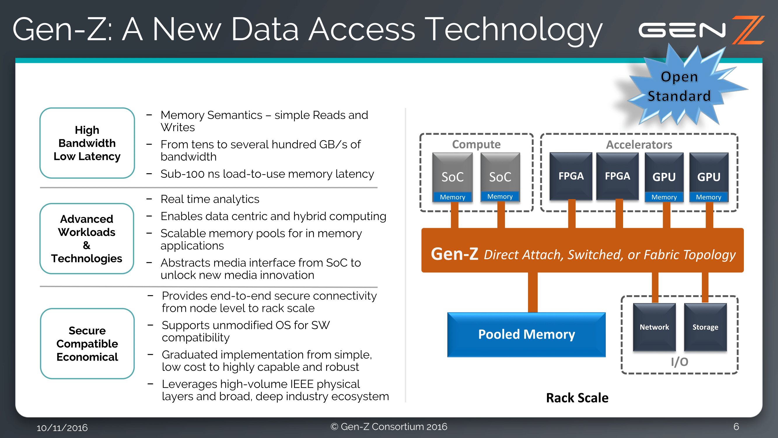
The interconnect is also aimed at offering real-time analytics, working between CPU cores, SoCs, FPGAs, GPUs, pooled memory and networked storage. There is also aims for security, as well as support via unmodified operating systems (which indicates that the new interconnect is a pure hardware design) and support within tiered memory hierarchy. Another goal is low-cost implementation, which will require working close with semiconductor manufacturers.
The Consortium consists of a number of key players designing SoCs and large scale systems:
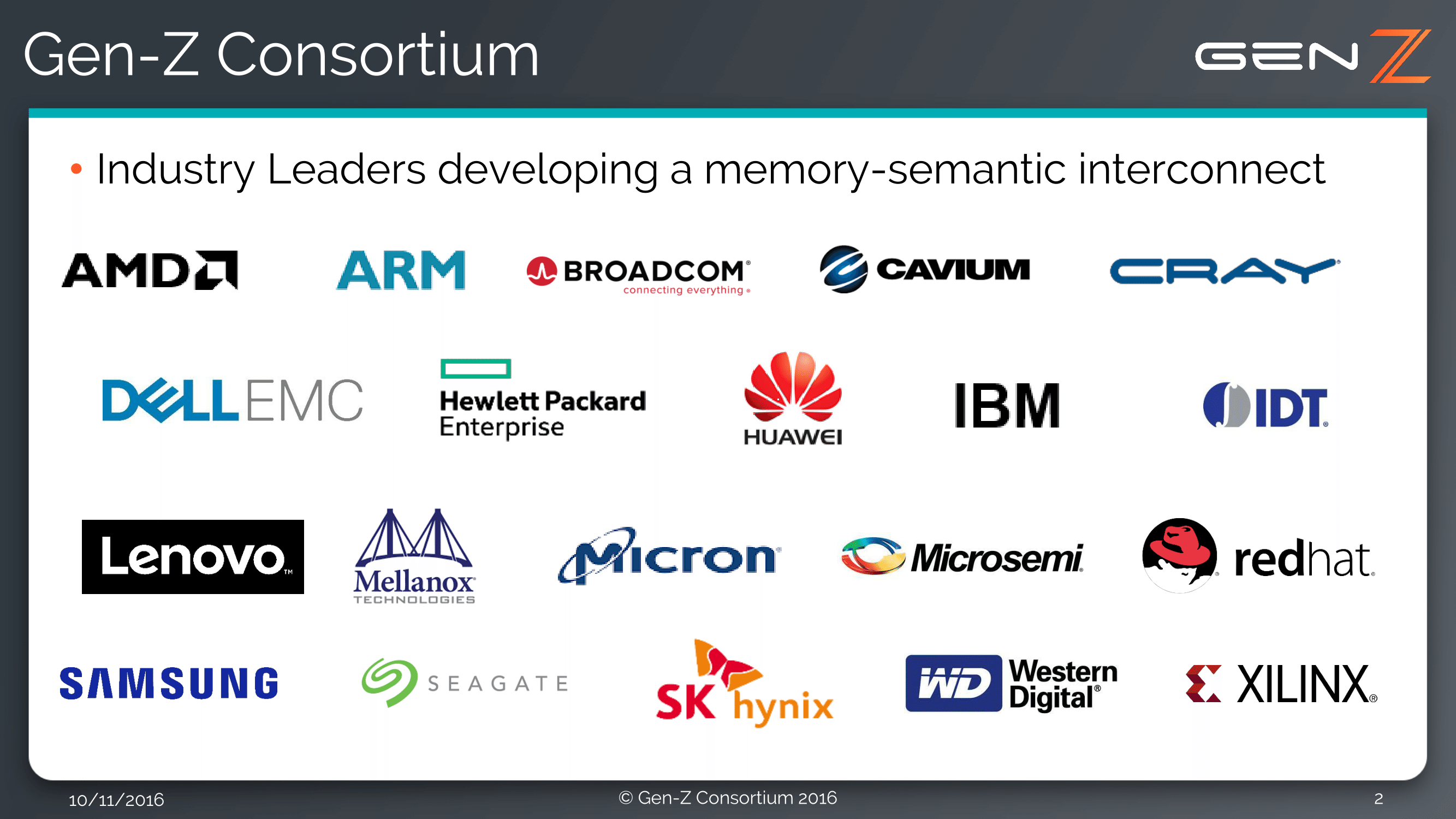
Among the IP vendors (ARM, IBM) are fabless semiconductor companies (Broadcom, Xilinx) and big enterprise players (Dell EMC, HPE, Cray for supercomputers). Any which way you cut it, it represents a lot of the industry, except one major player at least – Intel. Despite Micron in there with 3D XPoint, Intel’s own designed interconnects are under lock-and-key with patents and proprietary technology, and given how the enterprise market is moving more into accelerators and/or non-x86 architectures with a myriad of microarchitectural designs, solution providers have more options to choose from. That being said, with the goal of Gen-Z to be open and free, that doesn’t stop anyone else from actually using it and it would be argued that the ultimate goal is to promote adoption.
Despite this week being the formal announcement of the Gen-Z Consortium, it would seem that something has been brewing for a while given that the press release today has stated that the core specification covering the architecture and protocol will be finalized in late 2016. I suspect we might hear something at SuperComputing 2016 in mid-November.
Source: Gen-Z


15 Comments
View All Comments
MrSpadge - Monday, October 17, 2016 - link
> A single fiber has vast bandwidth. If limited by cost and present technology, adding more cables quickly solves the problem.Besides more fibers an optical transmitter requires light sources, modulators and detectors, as well as packaging of all components. There's no fully integrated reasonably cheap solution in sight yet, despite people working on it since at least 15 years. That doesn't mean it won't happen, but it takes a lot more than "simply attach a few more fibers".
Visual - Thursday, October 13, 2016 - link
So what is this thing in human words?Replacement for FSB/HyperTransport/QuickPath? But it talks about various storage devices and not just CPU and RAM... so is it going to replace PCI-express too? Or is it just a protocol thing that will work on top of PCI-e? DMA replacement of sorts?
vanilla_gorilla - Thursday, October 13, 2016 - link
My assumption is that this is designed to support the coming storm of storage class memory.tuxRoller - Saturday, October 15, 2016 - link
It's a bit of everything.Right now it is a packet based protocol that uses memory semantics across an 802.3 phy with connections between points composed of lanes (up to 256). Each lane has a signalling range of 16-112 GT/s, and lanes are aggregated into links, with the possibility of multiple links per connection. Supported topologies are point to point, daisy-chained or switched, with discrete and integrated packaging possibilities.
Devices are located on subnets (each of which supports up to 4k devices), and a network can be composed of up to 64k subnets.
They are also in the process of specifying a new connector (and the requirements they have for that connector are insane).
So, it's really designed for very, very large numbers of processors, with accelerators as first class citizens, and vast amounts of storage (DRAM, nvm, and cold storage). That means it's competing with this kind infiniband, but, interestingly, it can also be integrated so as to replace those buses you mentioned.
lanek81 - Thursday, October 13, 2016 - link
Is there a reason why AMD have been removed completely from each part where it was cited in the original press release ?And obvliously, it seems Gen-Z, is AMD Global memory Interconnect ( GMI link, or data coherent fabric )